Elephantech Unveils HDI Microvia Formation Process Using Copper Nanoparticle Ink
– A Novel Solution for High-Density Board Manufacturing –
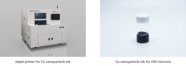
December 23, 2025, Tokyo, Japan – Japanese deep-tech Elephantech announced successful development of an innovative process to form High-Density Interconnect (HDI) microvia leveraging the company’s copper nanoparticle ink, named “Cu Nano Direct Plating.”
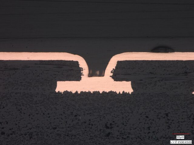 Blind via formed using Elephantech’s copper nanoparticle ink (MSAP)
Conventional BVH formation via electroless copper plating presents several shortcomings:
In order to address these challenges, Elephantech has developed a novel direct plating process using its proprietary advanced copper nanoparticle ink.
Technology Overview
This technology enables copper seed layer formation in BVHs by combining the application of copper nanoparticle ink with aqueous reduction treatment.
After desmear processing of the vias, a copper nanoparticle ink coating is applied. As the newly developed copper nanoparticles are engineered to adsorb onto the via sidewalls, upon drying, the nanoparticles align on the inner walls of the vias.
Subsequently, immersion in a reducing solution removes the oxide film on the nanoparticle surface, allowing them to form a continuous, uniform copper layer.

Process illustration (MSAP/Subtractive)
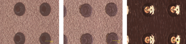 (from left) after drilling – after inkjet printing – after electroplating (MSAP・conformal)
With this process, the reducing solution serves as an alternative to chemical plating, enabling a significantly simplified flow while offering enhanced process stability and greater design flexibility. By employing a reducing solution that does not generate hydrogen, it eliminates outgas from the underlayer. As a result, the risk of gas-induced voids is fundamentally eradicated to achieve palladium-free and formaldehyde-free engineering.
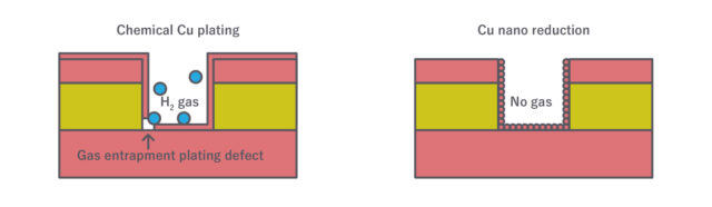 Comparison of Cu nano reduction VS electroless plating
By replacing electroless plating with “copper nanoparticle ink coating + reduction” solution, the technology is applicable to a wide range of manufacturing methods across SAP, MSAP, subtractive and full additive. Additionally, the ink, as an inkjet-printable material, supports both selective and full-surface deposition.
The mechanism of the process is that copper nanoparticle ink penetrates deeply into the micro-scale surface irregularities of the via sidewalls and adheres firmly to them. Owing to their miniaturized particle size of 15 nm, the nanoparticles carry high surface energy. The force that reduces surface energy by driving the nanoparticles onto the via walls, and the force that pulls nanoparticles toward each other maintain a well balance, sustaining a state where the nanoparticles adsorb to the via walls without aggregation. Such behavior is realized on both glass and epoxy substrates.
While other processes require a seed layer removal step, Elephantech’s approach manages to eliminate it due to the homogeneous copper-copper interface formed between the inner-layer copper nanoparticles and the subsequently plated copper. Through a straightforward reduction and plating process, a robust electrical connection is created, ensuring reliable conductivity.
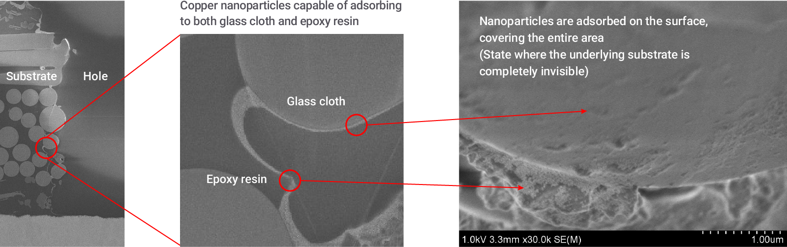
Cross-section SEM image of via inner wall after inkjet printing
Evaluation Results
Vias fabricated using this process have successfully passed the following thermal cycling test.
Test pattern
4-layer HDI (1-2-1 build-up)
Hole diameter (Top): φ0.1mm, Insulation layer (dielectric) thickness: 0.06 mm
Target plating thickness: 20μm
L1-L2 Via: 36 chains, L3-L4 Via: 32 chains
Temperature
1 cycle: -65°C (15 min.) / 125°C (15 min.)
Number of cycles: 700
Criteria: Resistance variation within ± 10%
Result: PASSED
After 700 cycles, the resistance variation remained minimal within the ±10% threshold. No abnormalities, including disconnections or cracks, were observed. All test requirements were successfully satisfied.
Outlook
Moving forward, Elephantech will advance commercialization of this BVH technology by supplying printing equipment and functional inks to PCB manufacturers.
With a stable mass-production process for the copper nanoparticle ink in place, samples are currently available to support customer evaluation. The technology is designed for integration into existing production lines, enabling manufacturers to assess its applicability for new via formation process.
Inquiries
Elephantech Inc> Inkjet Equipment and Material Business DepartmentSales Unit
ijs-sales-unit@elephantech.co.jp
Company Overview
| Name | Elephantech Inc. |
| Establishment | January 2014 |
| Headquarter | 4-3-8 Hatchobori, Chuo-ku, Tokyo 104-0032, Japan |
| Representative | Shinya Shimizu, Representative Director / CEO / Founder |
| Business Description | Development, manufacture and sales of proprietary machinery and materials, as well as PCB products |
| URL | https://elephantech.com/en/ |
Elephantech Inc. Public Relations: pr@elephantech.co.jp