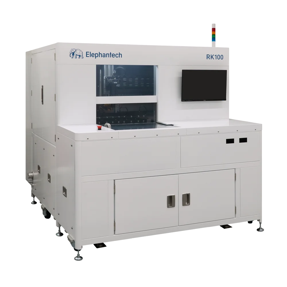
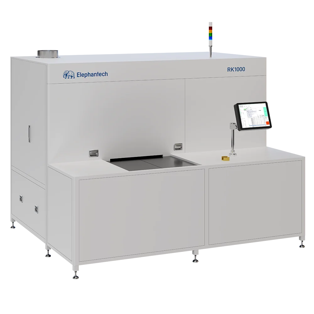
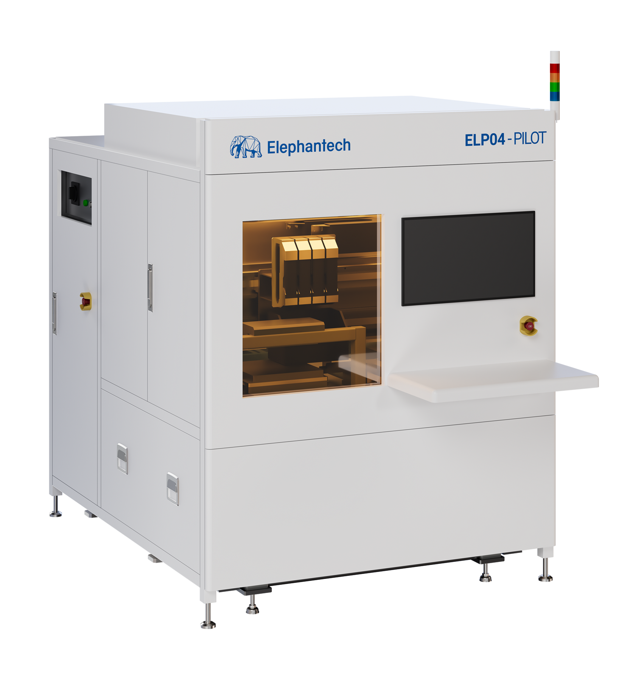
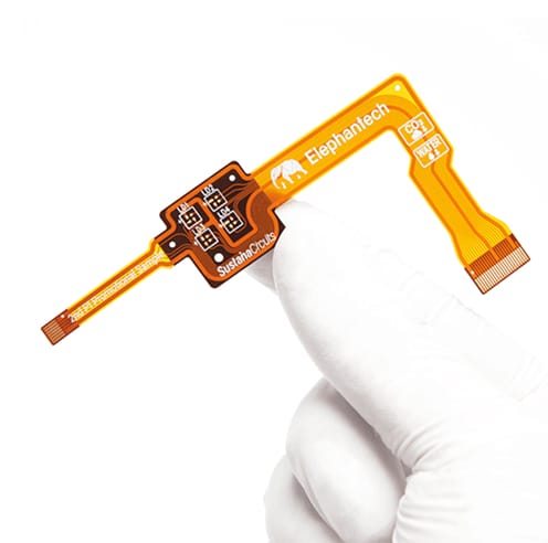
Our products SustainaCircuits

Our clean circuit boards help customers cut cost, time, and their environmental footprint.

SustainaCircuits™ are printed circuit boards made using our proprietary Pure Additive™ production process that fuses production efficiency and cost-effectiveness with significant environmental benefits.

We use only additive manufacturing methods to offer customers printed circuit boards that are just that—printed—and by doing so, are drastically reducing resource usage and carbon dioxide emissions compared to conventional printed circuit boards made using subtractive manufacturing methods. At the same time, our simple and efficient production process helps customers get the most out of their own resources—time and money.

Our goal is to use SustainaCircuits™ to offer customers in the electronics industry a significantly more sustainable manufacturing solution while ensuring business growth and reducing our own environmental footprint.

The benefits of using SustainaCircuits™

**The above results are based on in-house analysis and calculations that have been verified by a third party.

Discover the values and story behind our SustainaCircuits™ technology.

Why Elephantech?

SustainaCircuits™ in action

SustainaCircuits™ can be used in the same electronic devices as conventional printed circuit boards.

Product information

With the aim of decarbonizing the printed circuit board market, we’re continuing to develop and extend our technology to support production of a wide range of printed circuit boards. We’re currently able to mass produce single-layer flexible printed circuit boards (flex circuits) and are in the process of extending our capacity to include mass production of double-layer flex circuits and FR-4 rigid PCBs.

Single-layer flex circuit

Standard specs

  • Substrate: Polyimide (PI)
  • Copper thickness: 12 µm (guaranteed minimum). Available up to 35 µm
  • Minimum trace/space: 100/100 µm
  • Maximum outer dimensions: 223 x 393 mm
  • Minimum FPC connector pitch: 0.3 mm

At Elephantech, we’re always working to increase our production capabilities and strive to offer customers optimal solutions tailored to their needs and anticipated mass production schedule. We can easily work with specifications other than those listed above. Get in touch and we’ll come up with a tailored solution that meets your needs.

Innovative production that refuses to compromise on quality

At Elephantech, we believe production innovation and exceptional quality should go hand-in-hand. That’s why we designed our production method to ensure the same quality as conventional products while simultaneously offering customers greater efficiency and environmental benefits.

Products currently in development

At Elephantech, our goal is to eventually use our technology to offer production of all types of printed circuit boards and we’re currently in the process of developing a wide range of substrate manufacturing technologies to make this goal a reality.

Examples of products in our development lineup

Double-layer flex circuit

Standard specs

  • Substrate: PI (Polyimide)
  • Copper thickness: 3 to 35 µm
  • Minimum trace/space: 50/50 µm
  • Maximum outer dimensions: 500 x 415 mm
  • Minimum FPC connector pitch: 0.2 mm
Rigid printed circuit board

Standard specs

  • Substrate: FR-4 composite
  • Copper thickness: 3 to 35 µm
  • Minimum trace/space: 50/50 µm
  • Maximum outer dimensions: 500 x 415 mm

*The above are development values. Product specifications and design are subject to change without notice.

Mass production portfolio

Technology applications Applications for SustainaCircuits™ technology

SustainaCircuits™ are printed circuit boards made by printing metal nano ink directly onto the substrate using inkjet printing. As our SustainaCircuits™ production technology is compatible with a wide range of substrate materials, we expect to be able to adapt it to a wide variety of applications.

Application examples

1.Production of special specification printed circuit boards

Example: Long-length flex circuits for monitoring battery levels

In response to an increase in demand driven by a surge in electric vehicle production, we successfully applied our printing technology to the development and production of low-cost, long-length flex circuits for monitoring vehicle battery levels.

Example: Screen backlight boards

Print-based processing can be used to simplify the structure of components such as LED backlight wiring and metal heat dissipation boards, potentially speeding up the assembly process and lowering production costs.

Applications beyond printed circuit boards

Example: Post-processing of semiconductors and display manufacturing

Our high-precision, high productivity NeuralJet™ inkjet print processing technology can also be used in soldermask processing and OLED display manufacturing.

Example: Ultra-thin heater wiring

By applying our technology to ultra-thin heaters of several hundred nm to several μm—a product that is difficult to process with copper foiling and silk screen printing—these can potentially be produced at lower cost and greater productivity than comparative products made using vapor deposition processing.

3. Development of applied manufacturing processes using inkjet printing technology

Example: IMPC® (In-Mold Printed Circuits)

As our In-Mold Printed Circuits use film insert molding to integrate the circuit into a molded plastic component, they are thinner, lighter, and comprised of fewer parts than in-mold electronics produced using conventional methods.

Use the form below to contact us if you’re interested in product development using our technologies. We look forward to offering a solution tailored to your needs.