Nanomaterials Powering
AI Computing Making the world sustainable with new manufacturing technologies.
Transforming the Electronics Industry with SustainaCircuits
Conventional printed circuit board (PCB) manufacturing relies on etching copper-clad laminates to form conductive traces, which marks a subtractive approach long associated with resource inefficiency and hazardous byproducts. It consumes three to four times more copper than the circuit requires, uses large volumes of water, and generates wastewater that demands extensive treatment.
PCBs made through these subtractive methods leave a substantial environmental footprint. For example, up to 30% of a smartphone's total carbon emissions come from its PCBs.1
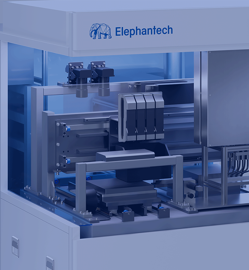
Elephantech’s proprietary additive process, SustainaCircuits, redefines how PCBs are manufactured to establish a new benchmark for the electronics industry.
PCBs made through these subtractive methods leave a substantial environmental footprint. For example, up to 30% of a smartphone's total carbon emissions come from its PCBs.1
Elephantech’s proprietary additive process, SustainaCircuits, redefines how PCBs are manufactured to establish a new benchmark for the electronics industry.
1: Aditya Joshi et al 2021 IOP Conf. Ser.: Earth Environ. Sci. 795 012028
-
 Decarbonizing PCBs for a Net-Zero FutureUsing 70% less copper and achieving a 75% reduction in CO2 emissions, SustainaCircuits streamlines the entire PCB manufacturing flow from material input to utility consumption.
The result is a high-performance, cost-efficient PCB with a significantly smaller environmental footprint, matching the quality of conventional products while surpassing them in sustainability.