JVA2021 Award Ceremony: A short speech by our CEO, Shinya Shimizu.
- This article is more than 2 years old since it was last updated. The content may be outdated.
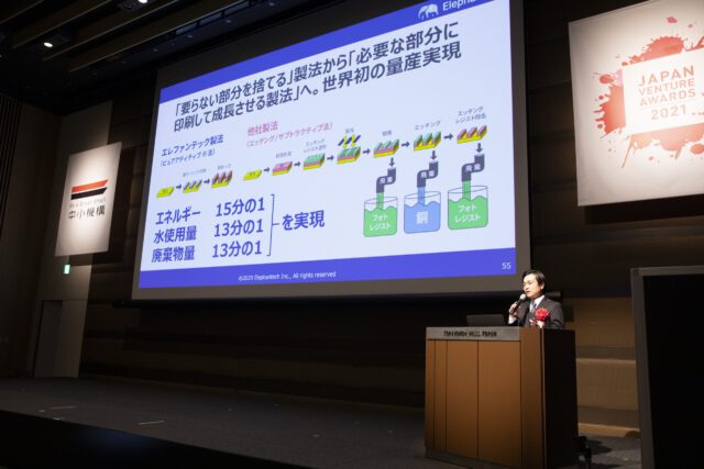
Here is a short speech from our CEO, Shinya Shimizu, at the “Japan Venture Awards 2021” ceremony held on March 1.

The electronics industry continues to grow rapidly on the back of global trends such as IoT and 5G. Under such circumstances, the industry’s impact on the environment has become a pressing concern. For instance, it wasn’t long ago that Shenzen in China was considered a hub for electronics and manufacturing industries. And yet, electronic circuit factories can no longer be built in Shenzen for environmental reasons.
The result of factories not being built in the coastal areas of China is that they are now being built in inland China and India. In other words, what we are seeing today is that the electronics industry, which is bad for the environment, is being moved to areas with looser environmental restrictions.
But is doing so really sustainable?
The electronics industry is reputed to be bad for the environment, but couldn’t we transform it into something more environmentally friendly?
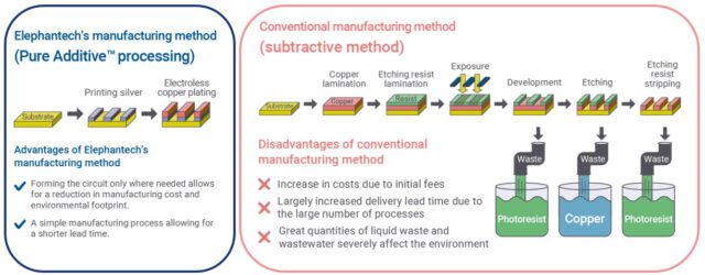
Up to now, the electronics industry has used a manufacturing method that involves applying copper foil over the entire surface and then melting and discarding the unneeded parts. As a result, one to two tons of water is required per square meter of electronic circuit produced.
In contrast, we’ve developed a manufacturing method that takes the opposite route by only printing metals where necessary and have adapted the method for mass production. This has allowed us to make electronic circuits while cutting its environmental impact by more than 90% when compared to conventional manufacturing methods.
Furthermore, we have established our own mass production factory and our customers have started replacing their electronic circuits with our products.
Our mission is to see Elephantech’s environmentally friendlier manufacturing method become the world’s de facto standard for electronic circuit manufacturing by 2030 or 2035, thereby making the electronics industry more sustainable.
Shifting from “dissolving unnecessary parts” to “printing onto necessary parts”

Our process achieves the desired copper pattern by printing the metal onto film and growing it, not only forgoing the need for copper foil manufacturing and CCL manufacturing processes but also eliminating the need for the etching process to dissolve and discard the copper foil.