Elephantech Has Developed DeepVia™ HDI Solution for High-Aspect-Ratio Microvia Metallization Enabling Very High AR ≥ 3 : 1 to Advance AI computing
Elephantech Inc. announced the successful development of DeepVia™ HDI, a high-aspect-ratio microvia metallization solution based on its proprietary copper nanoparticle ink and inkjet printing equipment. This approach addresses the limitations of conventional metallization methods, enabling enhanced performance for AI server PCBs.
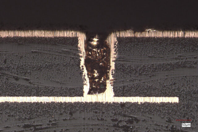 Cross-sectional view of metallized microvia
AR: 2.0, dielectric layer thickness: 200 μm, Φ: 100 μm
Background
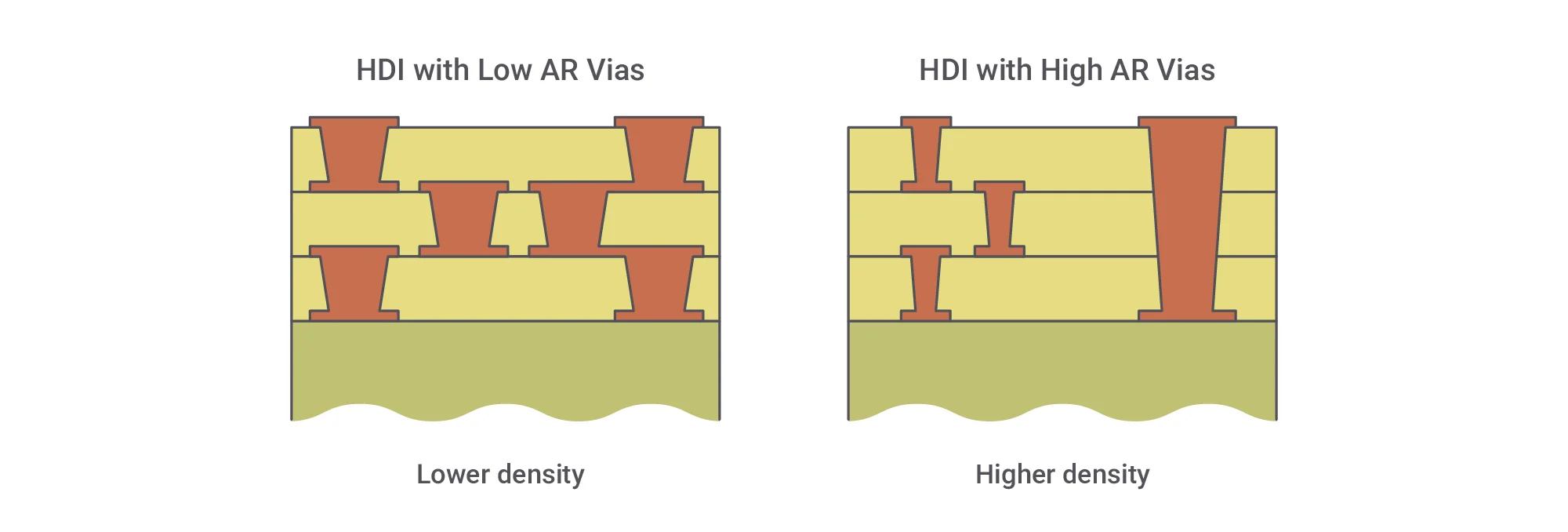
The rapid expansion of generative AI is driving demand for high-speed signal transmission and stable power supply at scale. As a result, AI server PCBs are evolving toward higher density and layer counts within limited form factors. Amid these trends, high-aspect-ratio vias are becoming essential to allow greater design flexibility and enhance system performance through efficient interconnection across deeper layers. However, conventional processes struggle to metallize such structures, limiting mass production capability. DeepVia™ HDI offers a novel solution to overcome the limitations and supports the realization of next-generation AI PCBs.
Challenges with Conventional Processes
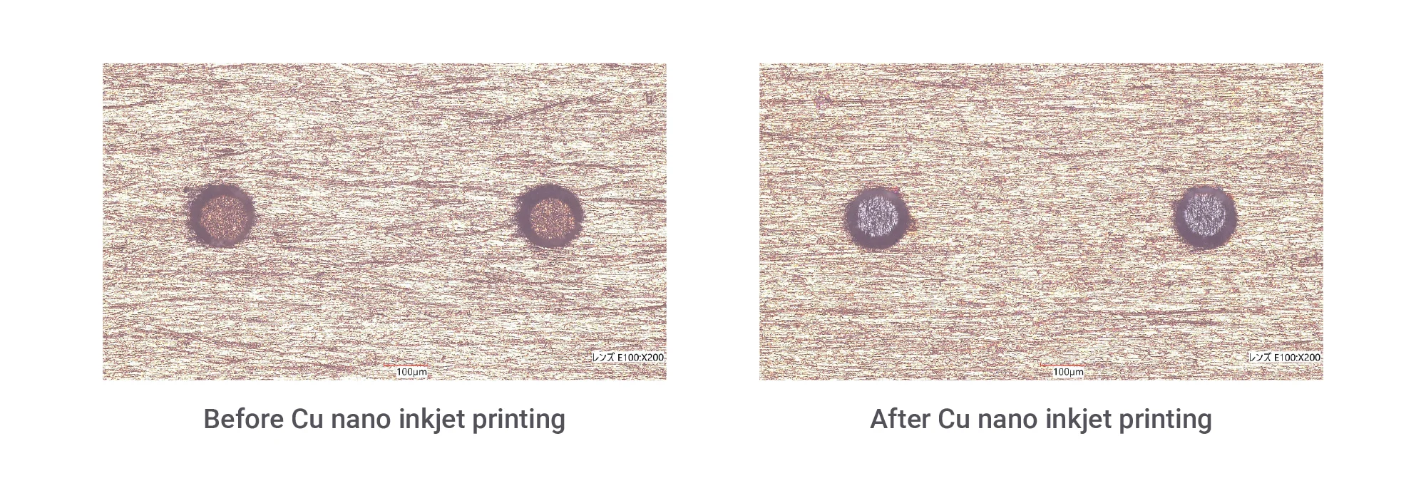
In general, vias in boards are formed along the process flow of drilling – seed layer formation – copper electroplating. Forming seed-layer is typically achieved by electroless copper plating.
During electroless plating, the board is immersed in an aqueous solution containing copper ions and reducing agents. The chemical reaction between the two materials deposits copper on the via walls to form the seed-layer. However, as the aspect ratio of the microvias increases, diffusion of the materials down to the bottom of the via becomes more difficult, leading to insufficient deposition. Therefore high AR microvias often suffer from incomplete seed-layer formation, posing a significant challenge in achieving high-performance AI servers.
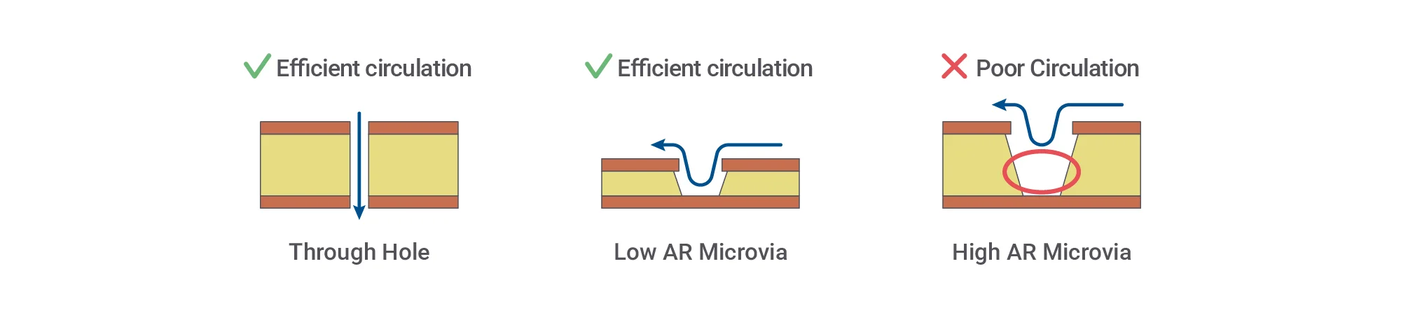 Impact of aspect ratio on solution circulation during microvia seed layer formation
DeepVia™ HDI Process Overview
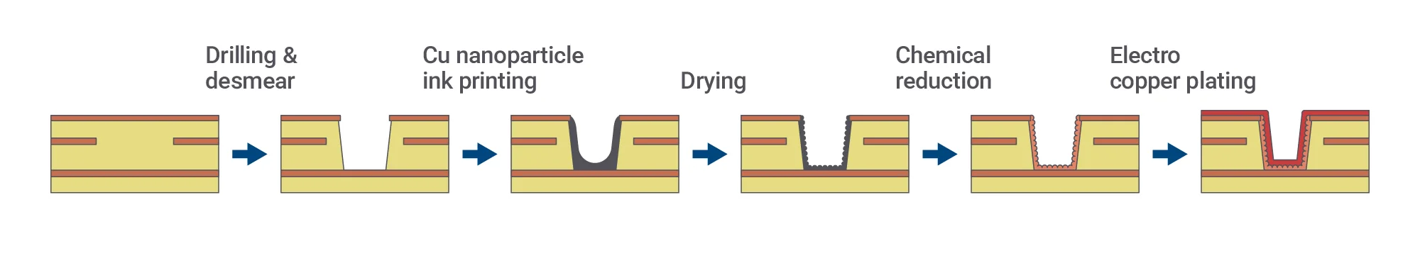
DeepVia™ HDI introduces a fundamentally different seed layer formation approach. Following drilling, copper nanoparticle ink is applied into the vias using inkjet printing. The ink, optimized for high AR via metallization, spontaneously spreads and wets the via surfaces, enabling uniform coating of the inner walls. In the subsequent reduction step, the deposited copper nanoparticles coalesce to form a continuous copper layer.
While copper electroless plating can be regarded as a process where copper ions and reducing agents are supplied simultaneously and continuously through solution circulation, DeepVia™ HDI decouples their supply. By doing so, DeepVia™ HDI solves the problem that copper ions + reducing agents’ reaction rates match the rate of solution transport, leading to consumption before the materials can reach the lower area of the deep via, and enabling effective seed layer deposition in greater depth of the structure.
Performance Comparison
| Approach | Max. aspect ratio range |
| Electroless copper plating (conventional) | 1.0 ~ 1.2 |
| DeepVia™ HDI | 3 ~ 4 |
DeepVia™ has demonstrated successful metallization of prototype microvias with very high aspect ratios (AR ≥ 3.0), representing a significant advancement over conventional electroless copper plating, which is typically limited to AR < 1.0, with practical limits at around 1.2.
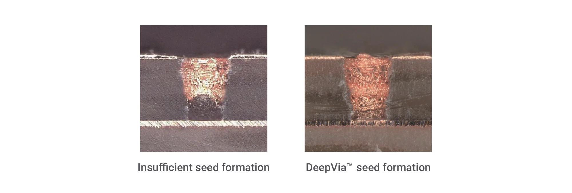 Comparison of seed layer formation prior to electroplating
Φ: 100 μm, AR: 2.0
DeepVia™ HDI has also been applied to coat extremely deep vias of 6 mm, effectively overcoming the aspect ratio constraints in the ink coating step. Although other process steps may still limit the full via fabrication, the primary challenge of inner wall coating has been eliminated.
Reliability test results
HDI specification
Φ(bottom): 0.1 mm, dielectric thickness: 0.2 mm, target plating thickness: 20 μm.
Temperature: −55 °C (15 min) / 125 °C (15 min)
Cycles: 100 (ongoing)
Criteria: resistance variation within ±5 %
Result: Pass
After the test, the change in resistance remained within criteria, and no abnormalities such as open circuits or cracks are observed, confirming stable interconnection reliability.
Key Technology: self-adsorbing copper nanoparticles and self-wetting ink
The breakthrough is built on the HDI microvia formation technology released by Elephantech last year. The key innovations enabling DeepVia™ HDI are self-adsorbing copper nanoparticles and self-wetting ink design. As aspect ratio increases, inkjet deposition of the ink alone becomes insufficient to achieve uniform coverage throughout the via, making control of ink transport necessary.
DeepVia™ HDI addresses this by specifically engineering a self-wetting ink that spontaneously spreads within the via. Through dynamical interactions with the prepreg surfaces, the copper nanoparticles sequentially adsorb and adhere onto the via walls, ensuring the ink’s self-spreading behavior. As a result, a uniform coating is formed even in very high AR structures. By precisely controlling ink deposition volume, reliable via metallization can be achieved.
Outlook
Elephantech will provide the key components of this technology, copper nanoparticle ink NCT-05 for high AR vias and inkjet printing equipment DK series to PCB manufacturers. Several validation cases with leading manufacturers are underway, with equipment deliveries scheduled within this year.
Inquiries
Sales Unit, Inkjet Equipment and Material Business Department, Elephantechijs-sales-unit@elephantech.co.jp
Company Overview
| Name | Elephantech Inc. |
| Establishment | January 2014 |
| Headquarters | 4-3-8 Hatchobori, Chuo-ku, Tokyo 104-0032, Japan |
| Representative | Shinya Shimizu, Representative Director & CEO |
| Business Description | Development, manufacturing, and sales of proprietary equipment and materials, and PCB products. |
| URL | https://elephantech.com/en/ |
Elephantech Inc. Public Relations: pr@elephantech.co.jp