Elephantech Develops DeepVia™ Silicon: A High-Aspect-Ratio Seed Layer Solution for 3D Semiconductor Integration A Novel Approach for Silicon Via Seed Layer Formation Addressing Increasing Aspect Ratios
Elephantech Inc. has developed a novel approach for forming copper seed layers in high-aspect-ratio (AR) silicon vias, utilizing proprietary copper nanoparticle ink and inkjet printing equipment. This technology contributes to solving the physical limitations of existing processes, which present significant challenges in next-generation 3D semiconductor integration.
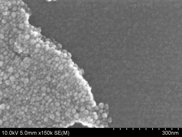
Cu nanoparticle adsorption state on Ti film (top-view SEM, ×150k, before sintering)
Background
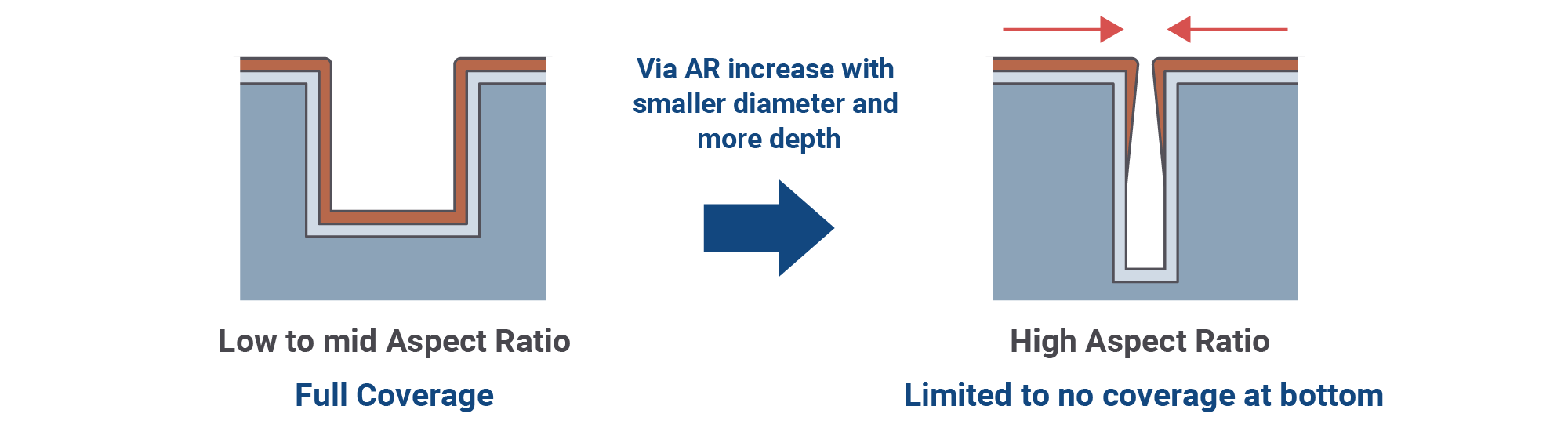
As AI accelerator performance continues to advance, the demand for higher density and smaller-diameter silicon vias in High Bandwidth Memory (HBM) and hybrid bonding is growing rapidly. Furthermore, as 3D integration architectures evolve—where multiple dies are vertically stacked—the required interconnect depth for silicon vias is increasing. With both diameter reduction and depth increase progressing simultaneously, via aspect ratios are rising at a pace exceeding previous technology generations.
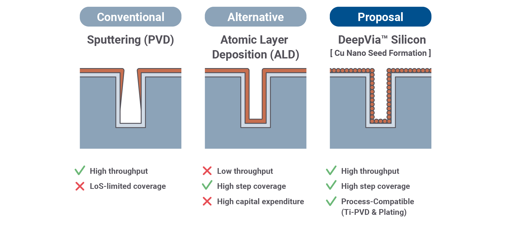
Challenges of conventional processes
In forming copper seed layers for high-AR silicon vias, the dominant industry process, Physical Vapor Deposition (PVD/sputtering), faces fundamental physical constraints due to the “line-of-sight” nature of sputtered particles. This makes it difficult to achieve uniform coverage at the bottom and along deep sidewalls as aspect ratios increase. There is a growing need for a new approach that achieves both uniform coverage and mass production compatibility.
DeepVia™ Silicon Overview
Elephantech has developed a novel process for forming copper seed layers on the inner walls of high AR vias, combining proprietary 15 nm-class copper nanoparticles with inkjet printing equipment. Copper nanoparticle ink is dispensed into the vias by inkjet printing, where proprietary adsorption characteristics enable uniform coverage of copper nanoparticles across the entire inner via wall surface. Through drying and sintering, the nanoparticles coalesce to form a thin copper film, which serves as a seed layer for standard electrochemical copper plating (ECP) to complete the interconnection.
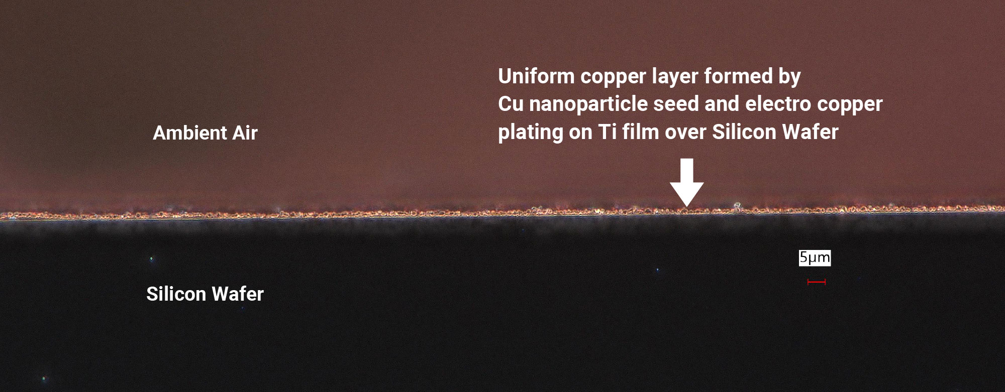
Cross-sectional SEM view of the uniform copper seed layer and electroplated layer over Ti barrier layer (Microscope, 1,000x)
※Process flow of the above prototype:
Ti barrier layer formation through sputtering → copper nanoparticle inkjet printing (ambient atmosphere) → sintering → copper electroplating
DeepVia™ Silicon Process
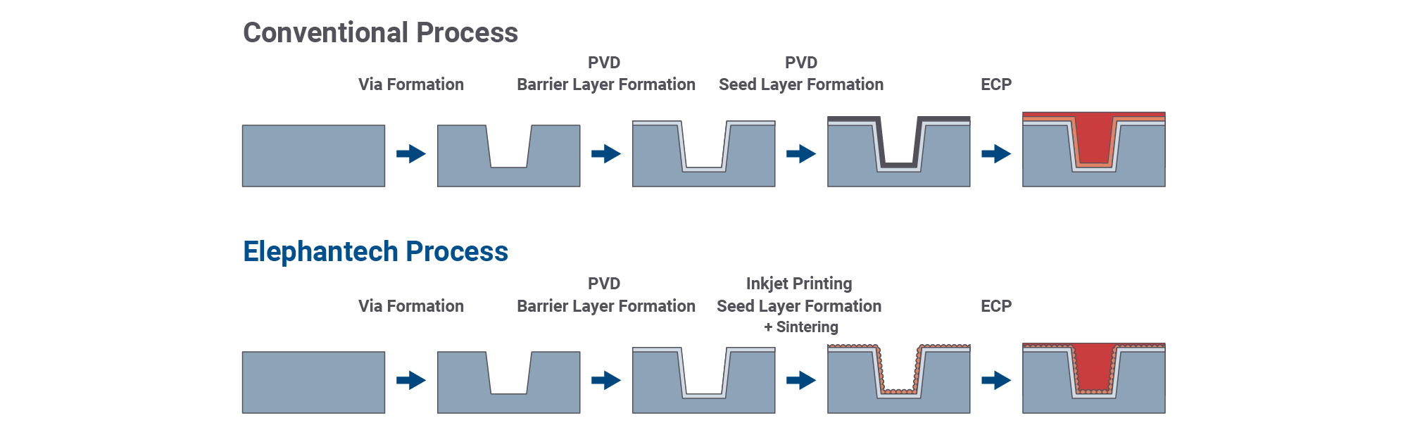
DeepVia™ Silicon not only serves as a complete replacement for the conventional PVD approach, but can also complement PVD as part of a hybrid solution to improve coverage.
Core Technology and Advantages
1. Distinctive Adsorption Behavior of Copper Nanoparticles
In typical nanoparticle deposition, particles often agglomerate into “islands”, making it difficult to form a continuous film. This island formation is a common challenge in thin film growth processes and is a factor that inhibits the formation of a continuous conductive path.
Elephantech’s 15 nm-class copper nanoparticles are engineered to self-assemble and adsorb densely onto the barrier layer (such as Titanium) without agglomeration. This characteristic enables the formation of a uniform, continuous seed layer.
SEM image of CuNPs’ adsorption state onto the Ti layer (before sintering)
2. Advantages of Inkjet printing
Existing dry processes (PVD, ALD) face limitations in addressing high-AR vias in terms of coverage or mass production compatibility, while wet processes also face barriers to mass production deployment. Spin coating is structurally limited in its ability to penetrate high-AR via interiors, while dipping presents challenges around bath management and waste liquid treatment in mass production environments.
Inkjet is the most promising process capable of simultaneously resolving these challenges. As an atmospheric pressure process, it offers a low barrier to integration into existing production lines, combining minimized material loss through selective deposition with stable process quality by eliminating the need for bath management. Compared to dipping, inkjet dispenses fresh liquid precisely where needed without creating a bath, enabling consistently stable seed layer deposition quality.
Outlook
Elephantech is currently conducting collaborative evaluations of this technology with memory manufacturers, foundries, and advanced packaging companies. Following verification of copper nanoparticle adsorption and plating connectivity on Ti (titanium) barrier layers, detailed evaluation is underway toward application to actual silicon vias, and Elephantech will accelerate the deployment of solutions addressing challenges in AI semiconductors. In addition to the currently demonstrated Ti (titanium) barrier layer, verification of applicability to other barrier metals including TiN is being pursued in parallel with customer evaluations.
For inquiries regarding evaluation and sample provision, please contact us at the address below.
Company Overview
| Company Name | Elephantech Inc. |
| Establishment | January 2014 |
| Headquarters | 4-3-8 Hatchobori, Chuo-ku, Tokyo 104-0032, Japan |
| Representative | Shinya Shimizu, Representative Director & CEO |
| Business Description | Development, manufacturing, and sales of proprietary equipment and materials, and PCB products. |
| URL | https://elephantech.com/en/ |
Elephantech Inc. Public Relations: pr@elephantech.co.jp