Elephantech Has Developed Copper Nano-Paste
SAphire™ G for Glass Vias in Advanced Packaging
Low-Shrinkage and Robust Metallization for High-AR TGVs
Elephantech Inc. has developed SAphire™ G, a copper nano-paste for Through-Glass Via (TGV) filling, utilizing its proprietary Self-Assembling Copper Nanoparticle (SA-CuNP) technology. The company has successfully demonstrated low-shrinkage, highly durable and robust metallization for high aspect ratio (AR) TGVs—a major bottleneck in the commercialization of glass substrates for advanced AI and HPC packaging applications. Joint evaluations with customers are currently underway. Through the provision of this product, Elephantech aims to accelerate the adoption of advanced semiconductor packaging and contribute to the evolution of AI computing.
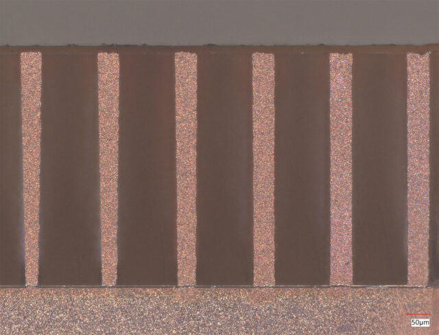 TGV cross-section after filling, sintering, and thermal shock testing with SAphire™ G
(Φ50 μm, 0.5 mm thickness, AR=10:1) (Microscope, ×300)
Background
As the performance of AI accelerators and other components increases, semiconductor packaging continues to advance toward higher density and larger form factors. Conventional organic substrates face emerging physical challenges, such as warpage due to thermal stress and limits on fine-pitch wiring formation caused by surface roughness. In contrast, glass substrates—offering a coefficient of thermal expansion (CTE) close to that of silicon chips and superior surface planarity—are expected to be a powerful foundation for advanced packaging. Glass is attracting significant industry attention not only for its low dielectric loss, which improves high-frequency signal transmission efficiency, but also for its high compatibility with future Co-Packaged Optics (CPO) technology.
However, practical application requires Through-Glass Via (TGV) conduction to electrically connect the top and bottom of the substrate. In particular, achieving reliable and cost-effective conduction in high-AR vias as density increases has become a major industry-wide bottleneck, creating a strong demand for innovative solutions.
Industry TGV Formation Trends and Technical Challenges
Two primary approaches are currently being considered for TGV metallization in advanced AI/HPC packaging: Electrolytic Copper Plating (ECP) and Paste Filling. However, both methods face significant hurdles for mass production as they adapt to high-AR vias.
While ECP allows for low-resistance metallization, it is difficult to deposit metal uniformly to the bottom of fine, high-AR vias, leading to poor via fill and compromised reliability. Furthermore, ECP requires long cycle times and complex liquid management. On the other hand, while paste filling offers a simpler process, conventional metal sintering pastes exhibit significant volume shrinkage during sintering, often leading to voids or gaps inside the via.
Additionally, silver (Ag)-based pastes face a significant cost barrier to mass production, with material costs approximately 60× those of copper. There is an urgent need for an innovative material that simultaneously achieves high performance, reliability, and cost-effectiveness.
Overview of SAphire™ G
Elephantech’s SAphire™ series of copper nanopastes is based on its proprietary SA-CuNP technology, where 15nm-class copper nanoparticles self-assemble onto the surface of micron-sized copper particles, allowing the entire structure to behave as a large nano-particle. This unique mechanism achieves excellent low-temperature sintering with a nano-particle content of only about 10 wt%, while minimizing residual impurities by reducing organic dispersants to less than 1 wt%.
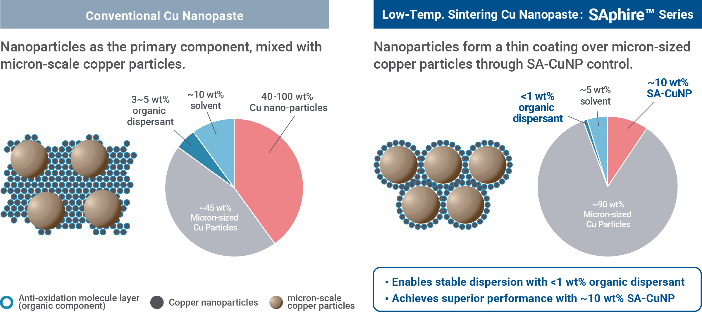
The new product, SAphire™ G, is optimized for TGV filling using this technology. By significantly reducing nano-particle content to minimize sintering shrinkage, it achieves metallization that suppresses voids and cracks in high-AR vias required for advanced packaging.
Technical Advantages
1. Highly Durable Metallization for High-AR Vias
Elephantech has achieved dense metallization in TGVs with a diameter of 50 μm and a thickness of 0.5 mm (AR=10:1). No cracks were observed following thermal shock testing (–50 °C ⇔ +125 °C, 250 cycles), confirming high metallization reliability.
2.High-Quality Filling and High Yield through Low-Shrinkage Characteristics
SAphire™ G suppresses the formation of voids and gaps caused by volume shrinkage during sintering. The low-shrinkage characteristics improve conduction reliability in high-AR via environments. They also reduce internal stress on the substrate during sintering, thereby minimizing the risk of damage and cracking in fragile thin glass. This contributes to improvement in production yields.
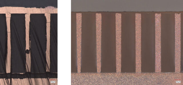
Comparison of TGV Cross-sections (Microscope, ×300)
・Left: Conventional copper nano-paste composed only of copper nanoparticles (post-sintering), numerous voids caused by shrinkage
・Right: SAphire™ G paste (post-sintering and thermal shock test), no voids or cracks even after thermal shock testing
*Specifications of sample and process flow
– Glass Material: Borosilicate glass (TEMPAX Float®)
– Via Specifications: Φ50 μm (AR=10:1)
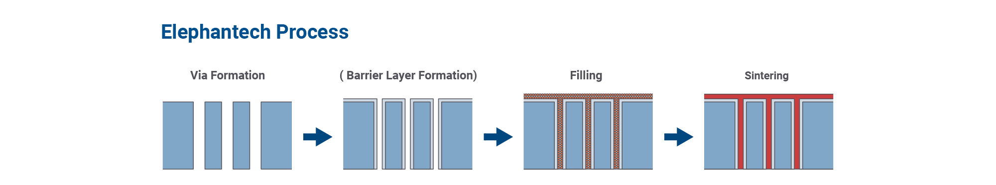
– Process Flow: TGV filling with SA-CuNP paste using an isostatic pressing → Sintering at 300 °C for 60 minutes
– Reliability Test: Thermal shock test conducted (–50 °C ⇔ +125 °C, 15 minutes each, 250 cycles)
3.Economic Viability at Scale
The simple fill and sinter process eliminates the need for seed layer formation and long processing times with complex bath/electrolyte management required by ECP. While using copper to keep material costs approximately 1/60 that of silver, SAphire™ G demonstrates the potential for conductive performance comparable to silver-based pastes.
Future Development
SAphire™ G is currently in the joint evaluation phase with domestic and international substrate manufacturers, glass panel manufacturers, and OSAT/packaging companies aiming for mass production of next-generation packages. We will accelerate reliability verification for practical use, targeting the glass core substrate market for AI/HPC and glass interposers for CPO. Guided by the concept “Nanomaterials Powering AI Computing”, Elephantech aims to solve semiconductor packaging challenges in the AI era through its unique nanomaterial technology.
Company Overview
| Company Name | Elephantech Inc. |
| Establishment | January 2014 |
| Headquarters | 4-3-8 Hatchobori, Chuo-ku, Tokyo 104-0032, Japan |
| Representative | Shinya Shimizu, Representative Director & CEO |
| Business Description | Development, manufacturing, and sales of proprietary equipment and materials, and PCB products. |
| URL | https://elephantech.com/en/ |
Elephantech Inc. Public Relations: pr@elephantech.co.jp