Elephantech Introduces DS-SAP™ for Fine Patterning on Semiconductor Package Substrates Dual-Seed Technology Enables Higher Density for Advanced AI Packaging
Elephantech Inc. has developed Dual-Seed Semi Additive Process™ (DS-SAP™), a novel process for semiconductor package substrates manufacturing. Through independently forming seed layers for surface patterning and via metallization, DS-SAP™ achieves both ultra-thin traces and reliable coverage of high-aspect-ratio vias. This breakthrough supports higher packaging density, helping accelerate the development of next-generation AI devices.
Background
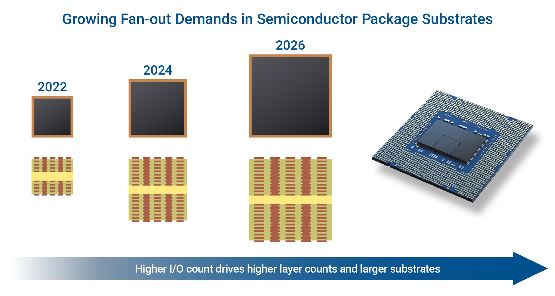
As AI workloads continue to expand, GPUs and CPUs are rapidly increasing their capability. As a result, semiconductor packaging has become a critical enabler of advancing computing performance, driving demand for unprecedented fine and dense conductor patterns on package substrates.
DS-SAP™ optimizes the Semi Additive Process, which is widely used for build-up layers in package substrates, overcoming its limitations toward ever-finer circuits formation.
Dual-Seed Semi Additive Process™
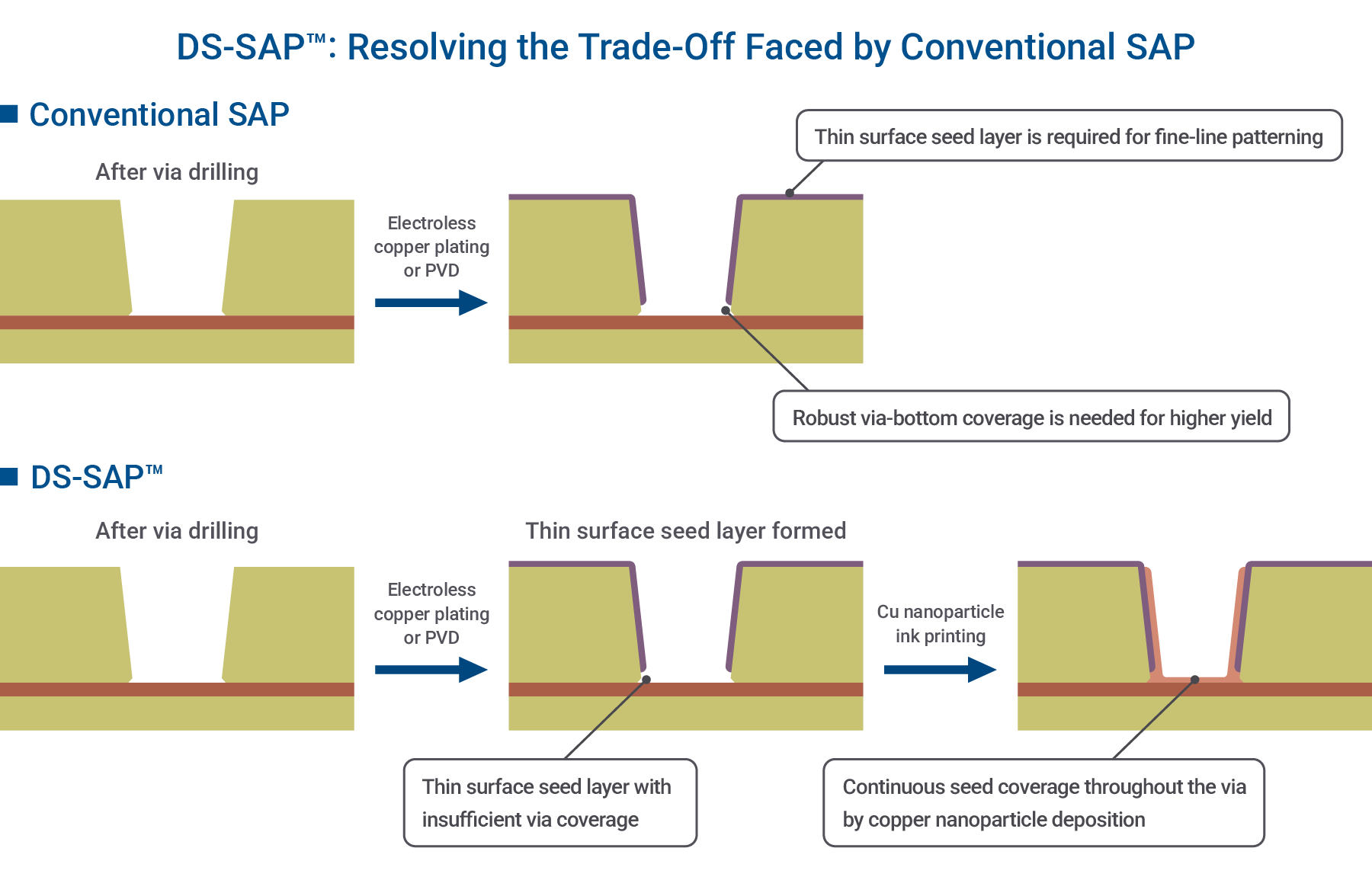
A typical SAP consists of the following steps: lamination, via drilling, copper seed layer formation by electroless plating, pattern plating, and seed layer removal. During the last step, part of the plated conductor is inevitably etched away as a side effect. Therefore, the thicker the seed layer, the longer etching times it requires, resulting in greater conductor loss and impeding achievable line width.
As conventional SAP deposits seed layers on both the surface and within vias simultaneously, it is infeasible to reduce the surface seed-layer thickness for fine circuits without jeopardizing continuity of the seed layer inside the vias, particularly at the via bottom. This makes an unavoidable trade-off between two conflicting requirements: an easily deposited thin surface seed layer and a difficult-to-deposit sufficient via seed coverage.
DS-SAP™ resolves this trade-off by separating seed layer formation in the two regions, achieving significant improvement of addressing both needs. Specifically, it firstly forms an ultra-thin seed layer on the surface using electroless copper plating or PVD, and then applies copper nanoparticle ink to the vias, complementing the insufficient seed layer to establish continuous coverage.
The solution is based on Elephantech’s proprietary copper nanoparticle ink, which provides a uniform layer inside the via, and its inkjet technology for selective deposition where additional seed formation is needed.
Application of DS-SAP™
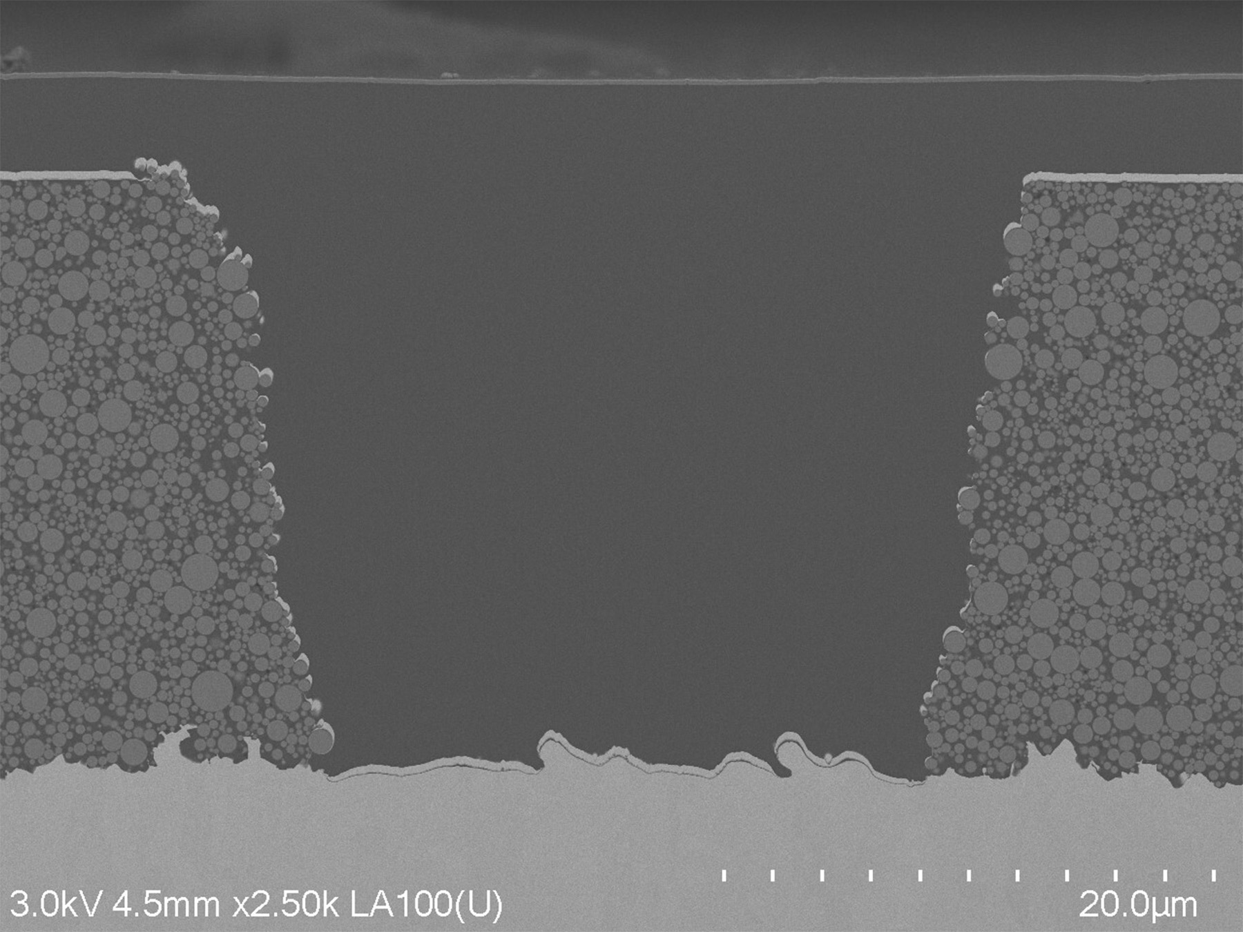
DS-SAP™ works in combination with either electroless copper plating or PVD approach to deliver effective results. The below cross-sectional SEM image illustrates its application to a PVD process. While a relatively thick seed layer is deposited on the surface, inside the via the seed layer remains discontinuous, causing insufficient seed coverage.
The samples were subsequently processed using electroplating alone (left) and DS-SAP™ copper nanoparticle ink printing + electroplating (right), with the respective results shown below. With the DS-SAP™ approach, the electroplated copper can be observed to grow continuously throughout the via without interruption.
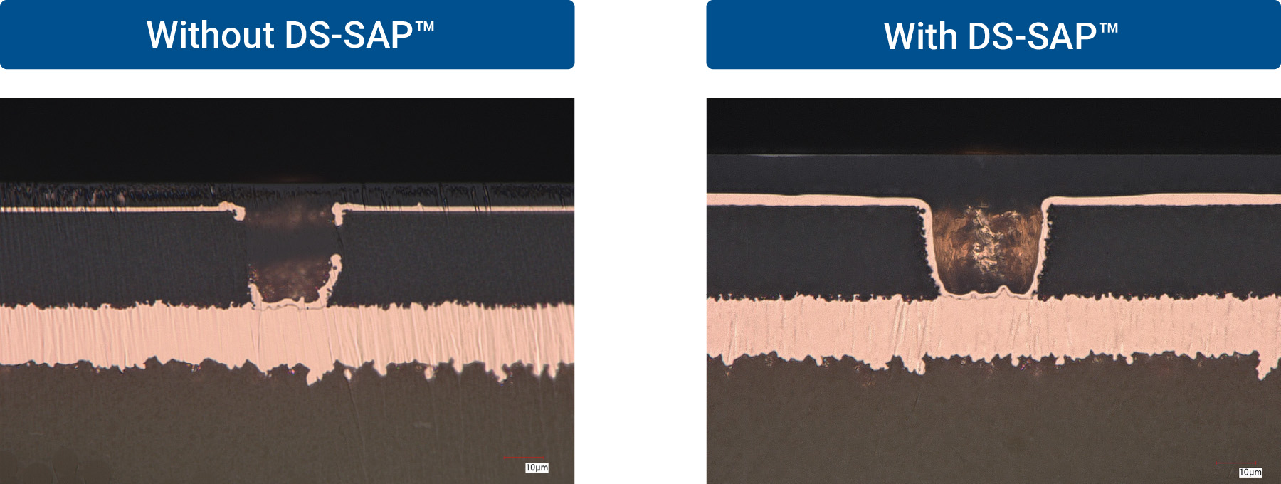 Cross-section after thin copper plating.
Interlayer dielectric film: ABF® GL-102, Via bottom diameter: 25 μm
ABF® is a registered trademark of Ajinomoto Co., Inc. in Japan and/or other countries.
Advantages
Adopting DS-SAP™ for semiconductor package substrate manufacturing offers the following advantages:
- Achieves fine L/S patterning
- Supports higher interconnect density through high-aspect-ratio vias
- Improves fan-out efficiency, reducing required build-up layer counts
Outlook
Elephantech has initiated evaluations of DS-SAP™ with several AI semiconductor manufacturers and advanced packaging companies. By supplying the proprietary copper nanoparticle ink and the inkjet equipment that enables the solution, the company is actively promoting deployment of the technology, aims at accelerating continued evolvement of AI hardware.
Inquiries
Sales Unit, Inkjet Equipment and Material Business Department, ElephantechCompany Overview
| Name | Elephantech Inc. |
| Establishment | January 2014 |
| Headquarters | 4-3-8 Hatchobori, Chuo-ku, Tokyo 104-0032, Japan |
| Representative | Shinya Shimizu, Representative Director & CEO |
| Business Description | Development, manufacturing, and sales of proprietary equipment and materials, and PCB products. |
| URL | https://elephantech.com/en/ |
Elephantech Inc. Public Relations: pr@elephantech.co.jp