Elephantech Unveils General-Purpose Multilayer PCBs With SustainaCircuits™ Technology
Overview
December 17, 2024, Tokyo, Japan – Elephantech has been mass-producing SustainaCircuits™, innovative printed circuit boards (PCBs) that reduce copper usage by 70-80% using printing technology. However, until now, we could only develop relatively niche single-sided flexible PCBs, which account for only about 2% of the market. The application to general-purpose multilayer PCBs2, which makes up 78%1 of the market, was highly anticipated but not yet realized, with plans for practical implementation after 2027.
We are pleased to announce that due to several technological innovations, we have successfully developed general-purpose multilayer PCBs earlier than expected. The main achievements are (1) compatibility with rigid substrates and (2) multilayer capability, enabling the replacement of the majority of PCBs worldwide.
This technology not only significantly reduces environmental impacts, including CO2 emissions, but also has the potential to reduce PCB manufacturing costs by over 1 trillion yen annually, primarily by reducing copper usage in general-purpose multilayer PCBs by 70%3, which constitutes a large portion of their cost structure.
We are already working with multiple electronics manufacturers and plan to start providing prototypes in the first half of 2025.
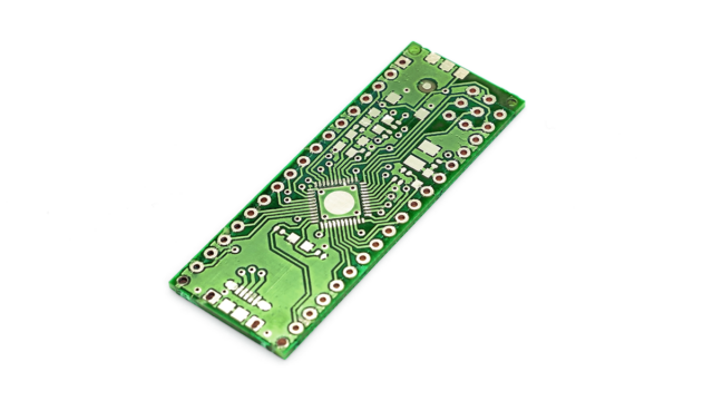 Photo of the developed general-purpose multilayer PCB (4-layer through-hole board)
- The market share data is based on area and includes semiconductor substrates. The figures are sourced from the 2023 Fuji Chimera Research Institute reports, 「FPCの注目アプリケーションと先端技術」&「エレクトロニクス実装ニューマテリアル便覧
- The definition of general-purpose multilayer PCBs refers to low-layer count rigid PCBs (RPCB) with 1, 2, 4, or 6 layers. This definition excludes build-up boards regardless of the number of layers.
- The typical value for copper reduction (mentioned as 70% in the original text) depends on the wiring pattern and is based on Elephantech’s research
Details of the Technology
Rigid Substrate Compatibility
We have developed a primer and copper nanoparticle ink that adhere strongly to FR-4.
Our printing method requires printing on smooth surfaces to achieve high adhesion, which has been disadvantageous from an adhesion standpoint. Insufficient adhesion has been the biggest challenge in adapting to rigid substrates.
The newly developed primer and copper nanoparticle ink for FR-4 demonstrates strong adhesion. Notably, they exhibit high heat resistance, which was previously difficult to achieve. After a 240-hour test at 150°C, they maintain an adhesion strength of over 1.0N/mm*, reaching a level suitable for use in rigid circuit boards.
*This is based on a test method in accordance with UL796 standards. The value is a reference measurement by Elephantech and is not a guaranteed value.
 Cross-sectional structure
Multilayer Capability
By developing a technology to apply ink inside vias and improving the primer, we can now form vias for multilayer wiring. We have successfully created 4-layer and 8-layer PCBs.
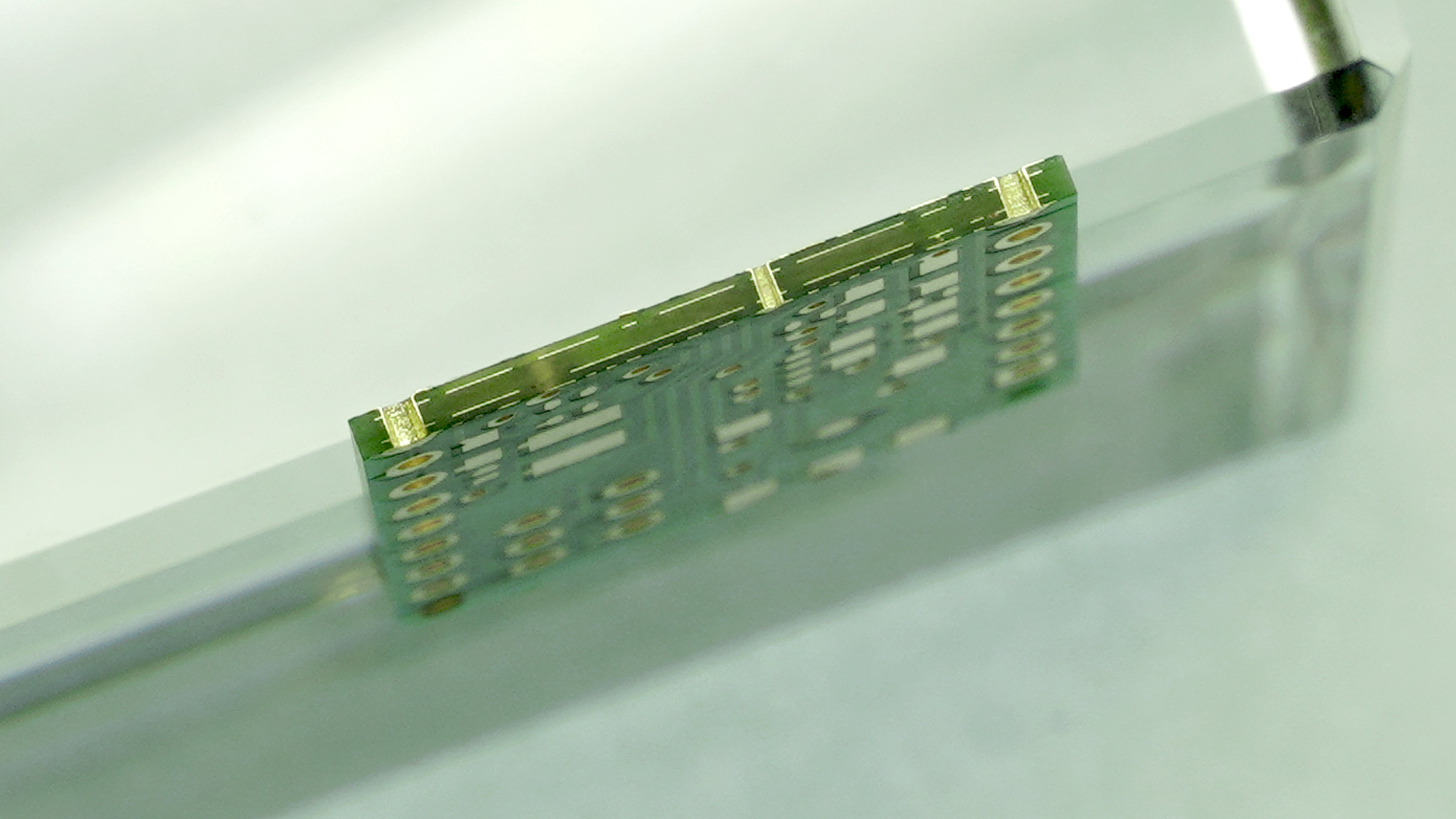 4-layer through-hole board
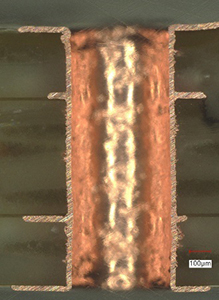 Cross section of 4-layer through-hole board
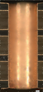 Cross section of 8-layer through-hole boar
However, the current materials and processes are for rigid boards and cannot be applied to multilayer film substrates at present.
Miniaturization
Through improvements in the combination of primer and ink, as well as enhancements in printing machine precision, we have achieved the capability to form wiring at an L/S of 50/50 μm. This represents a significant advancement from the previous L/S of 100/100 μm.
Achieving miniaturization requires that the ink does not spread on the surface of the primer; however, there was a challenge where primers that repel ink made drawing and adhesion difficult. With the newly developed primer, we have successfully ensured both drawability and adhesion while minimizing ink spreading to the greatest extent possible.
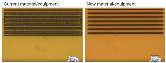 Comparison of Drawing Test Results at L/S = 50/50 μm
High Current Capability
The development of primers and inks with high adhesion and plating resistance has enabled the manufacture of PCBs with copper film thicknesses in the 100μm range.
Historically, in the world of printable electronics, the limitation on the amount of current that could flow has been a major challenge for widespread adoption. To address this, we have proposed a process combining printing and plating processes, but we were limited to copper film thicknesses of around 10μm. While this was sufficient for signal lines, it was inadequate for power electronics.
With the newly developed process, we can now achieve copper film thicknesses in the 100μm range through electroplating. As copper prices continue to rise steadily, the economic rationality of forming copper only where needed through plating increases as the copper thickness increases.
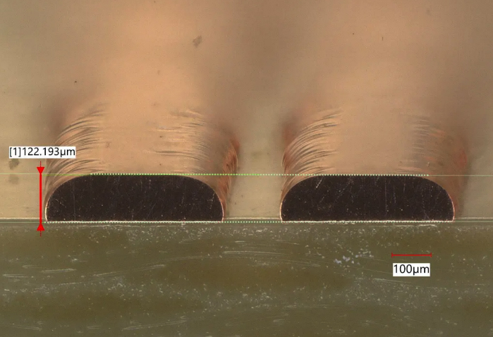 Wiring with thickness exceeding 100μm
Impact
Market Expansion
In the global PCB market, we have expanded from being able to address only about 2% of products on an area basis to now being capable of addressing 78%. While the market size for single-sided FPCs was around 10 million square meters, rigid boards with 6 layers or fewer account for 370 million square meters. Most electronic devices use rigid boards with 6 layers or fewer, and with this development, we can now replace almost all boards except for specialized ones.
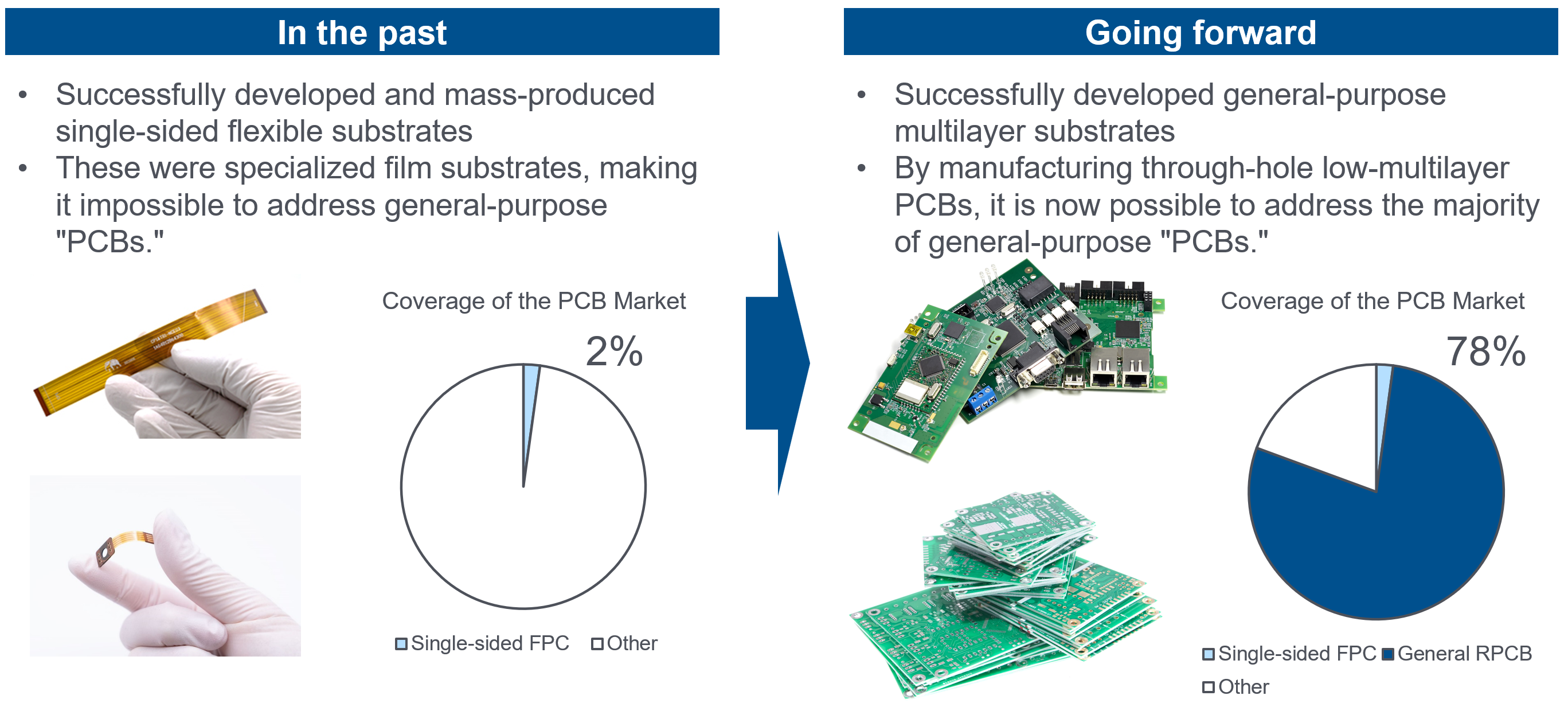
The percentages are based on surface area, including semiconductor substrates from the total.
The figures are sourced from the 2023 Fuji Chimera Research Institute reports, 「FPCの注目アプリケーションと先端技術」&「エレクトロニクス実装ニューマテリアル便覧
General-purpose multilayer PCBs are defined as low-multilayer RPCBs with 1, 2, 4, or 6 layers. Build-up PCBs are excluded regardless of the number of layers.
Process Reduction
The process reduction impact is even greater for multilayer PCBs than for single-sided PCBs, as our new method can form vias and wiring simultaneously.
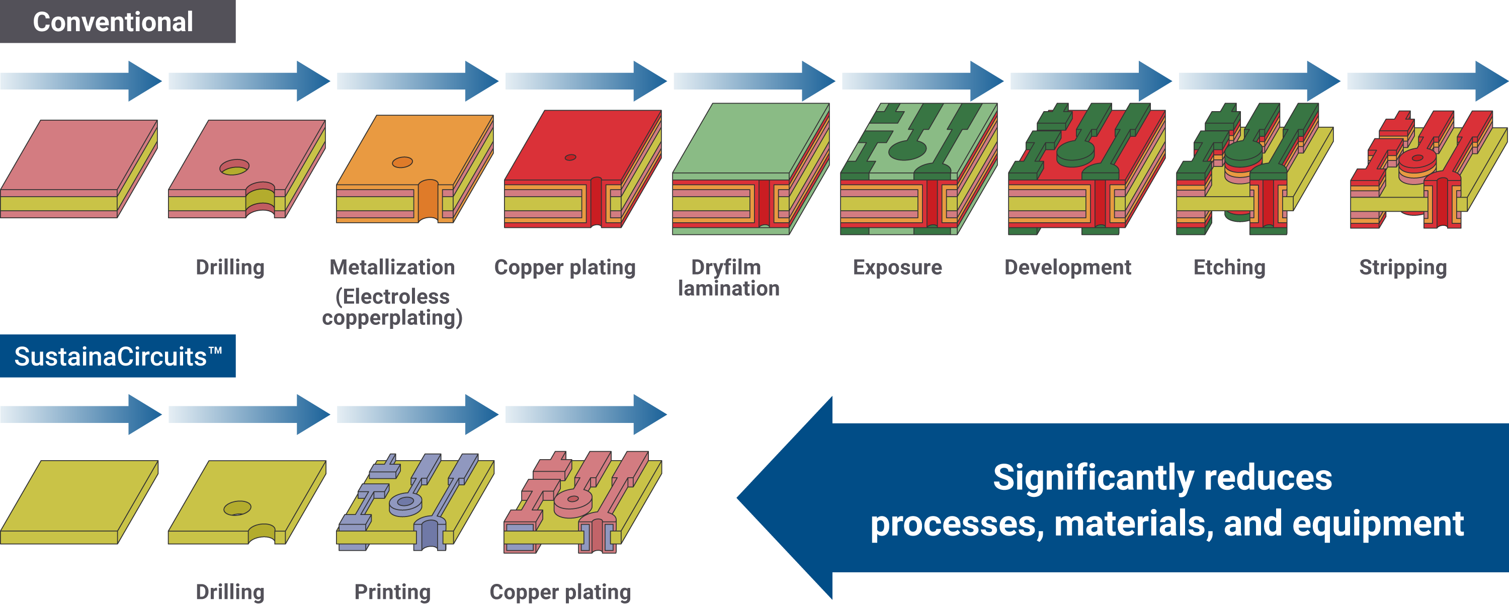 Comparison of manufacturing process for 2-layer PCBs
 Manufacturing process for 4-layer PCBs
Reduction in Copper Consumption
The resource with the most significant reduction impact through this method is copper. In the case of multilayer PCBs, copper consumption is substantial because copper foil is required for each layer, and through-hole plating also consumes copper.
In contrast, our method involves a process that grows copper only where necessary. While dependent on the pattern shape, this typically enables a reduction in copper usage by about 70%. For the newly developed general-purpose multilayer PCBs, we estimate a global copper cost reduction potential of around $6.7 billion.
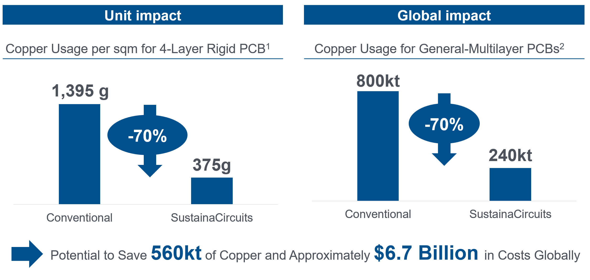
- The conventional method assumes an inner copper foil thickness of 35μm, outer copper foil thickness of 18μm, and plating thickness of 25μm.
- Based on the 2023 Fuji Chimera Research Institute‘s “エレクトロニクス実装ニューマテリアル便覧“. The estimated market size for electrolytic copper foil for general FR-4 in 2029 was combined with the market size for copper used in plating. Plating assumes a thickness of 25μm.
- Costs are based on the price of copper foil, not raw copper. Calculations use the November 2024 benchmark price of ¥1,448/kg for raw copper, plus the average processing cost for copper foil.
Next Steps
We are already prototyping test samples at our development site and have cleared major evaluation criteria. We plan to start providing prototypes in the first half of 2025 and establish mass production capabilities.
Printed circuit boards manufactured using our method can be mass-produced using existing manufacturing equipment, except for the printing process, by introducing our printing equipment into conventional general-purpose multilayer PCB manufacturing plants. For the supply system, we will consider both in-house manufacturing and providing our equipment and materials to partners.
Expected Scope of the Developed Technology
| PCB type | Multilayer plated through-hole board |
| Substrate type | FR-4 |
| Minimum L/S | 50/50 μm |
| Minimum via/land | Φ0.15 mm |
| Via type | PTH, IVH |
| Cu pattern thicknes | 10 – 100µm |
| The number of layers | No specific technical limitations |
| Size | No specific technical limitations |
| Surface treatment | No specific technical limitations |
Company Overview
| Name | Elephantech Inc. |
| Establishment | January 2014 |
| Headquarters | 4-3-8 Hatchobori, Chuo-ku, Tokyo 104-0032, Japan |
| Representative | Shinya Shimizu, Representative Director & CEO |
| Business Description | Development of printed electronics manufacturing technology and provision of related services |
| URL | https://elephantech.com/en/ |