
Advanced Materials: from Nanoparticles to High-Performance Electronics
Elephantech’s technology begins with copper nanoparticle engineering. Through continuous R&D, we have established an integrated nanomaterials development framework encompassing nanopastes, conductive inks and primers. Together, these materials form a diverse portfolio that underpins Elephantech’s proprietary electronics manufacturing processes.
Nanomaterial Development
Elephantech integrates proprietary nanoparticle engineering and cutting-edge self-assembly control to fundamentally enhance the performance of advanced electronics materials.
Nanoparticle Engineering
Highly controlled copper nanoparticles with an average particle size of ~15 nm (D50 = 13.4 nm) are developed with a narrow size distribution. This uniformity eliminates the need for classification processes, enhancing manufacturing efficiency and material stability.
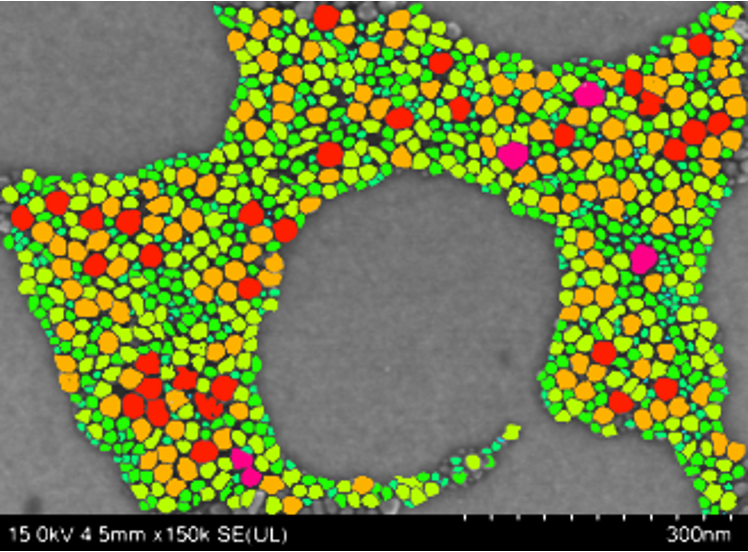
Copper nanofiller's SEM image
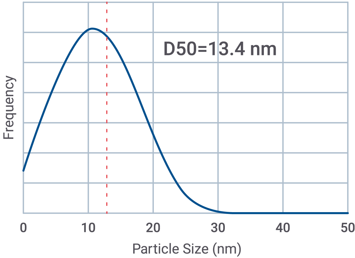
Copper nanofiller's particle size distribution
Self-Assembling Copper Nanoparticle Technology
A proprietary HDSM (High Density Small Molecule) surface treatment forms a high-density ligand layer (~6 molecules/nm²) on each nanoparticle. This surface engineering plays a critical role in controlling inter-particle interactions, providing the foundation for stable dispersion and enabling controlled self-assembly.
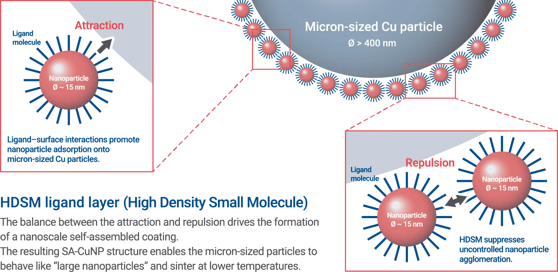
Building on the surface design, nanoparticles selectively and uniformly assemble onto target surfaces through a precisely balanced interplay of inter-particle repulsive and attractive forces.
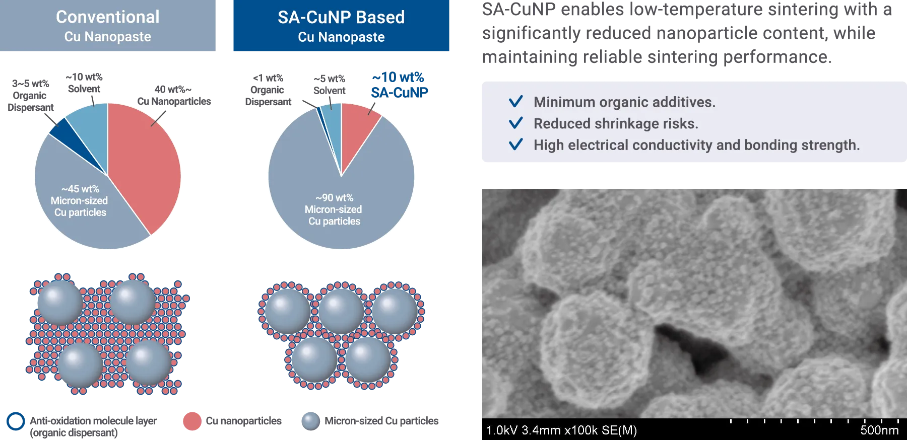
Comparison of SA-CuNP material design and conventional copper nanopastes.
This Self-Assembling Copper Nanoparticles (SA-CuNP) functionality provides greater flexibility in material design, particularly for sintering and viscosity control:
– Higher metal loading
– Improved sinterability, electrical conductivity and thermal conductivity
– Reduced gas generation and residue during curing
– Low-temperature sintering with improved adhesion and thermal stability
Powered by these technologies, the material supports multiple formats, represented by inks and pastes, broadening the design and manufacturing possibilities for electronics.
Copper Nanoink: Core for Nano Copper Deposition
As a direct application of the copper nanofiller, Elephantech’s self-wetting nanoink marks a key constitute of its unique Nano Copper Deposition, the disruptive manufacturing method for conductive seed-layer formation via inkjet printing.
The characteristics of the ink impact every step of the production chain: from storage, printing, to sintering and pattern formation. Its stability, particle size, solvent volatility, sinterability and adhesion to the substrate collectively determine conductivity, reliability and yield throughout the process.
Elephantech’s copper nanoink delivers industry-leading stability and processability, enabling both simplified manufacturing operations and consistently high-performance interconnects.
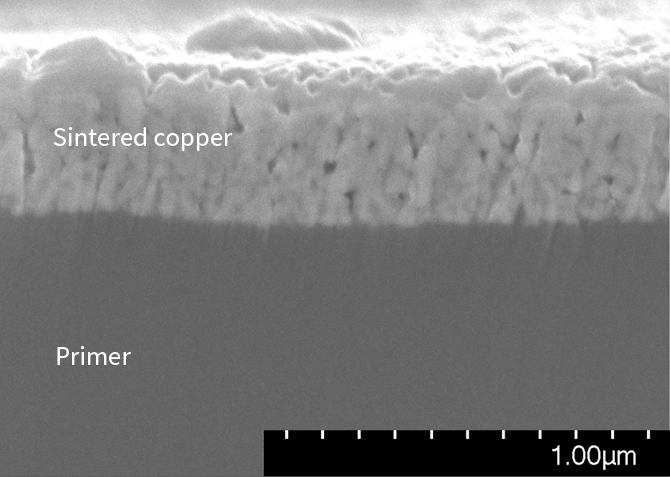
Cross-section SEM image of the ink-primer interface after sintering
Primer Technology: Dramatically Enhances Productivity
Complementing the nano ink, Elephantech’s uniquely formulated epoxy-based primer plays a crucial role in achieving reliable, fine-line circuitry through 3 mechanisms:
- Enhanced adhesion: The primer forms a strong physical bond between the ink and the base material, improving adhesion strength.
- Cross-material compatibility: With high affinity for the ink, the primer ensures smooth trace formation across diverse substrates from flexible films to rigid boards and glass.
- Droplet control: During the inkjet printing process, the pre-coated primer stabilizes droplet landing behavior, enabling precise, fine wiring patterns.
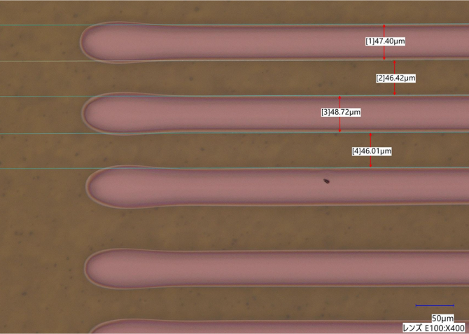
Minimized droplet landing diameter with controlled droplet behavior
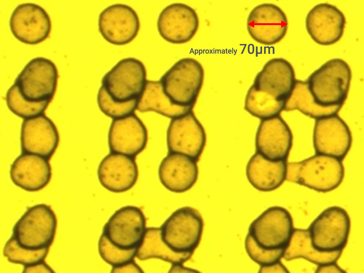
Fine-pattern formation challenged by adjacent droplet merging and shape distortion
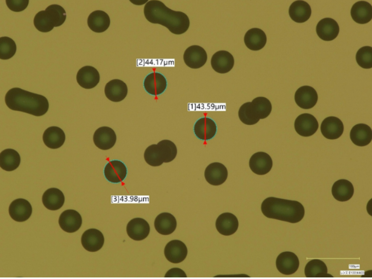
With primer applied, droplet merging and distortion are effectively suppressed, enabling fine-pattern formation
Material Analysis Technology That Ensures Quality Development
Advanced material innovation relies on deep analytical insight at the nano scale. From the early stage of research, Elephantech employs comprehensive analytical techniques to understand molecular behavior and root causes beneath the mysterious phenomenon of material science.
The findings serve as the foundation for the company to design particles with properties tailored for reliable electronics manufacturing.
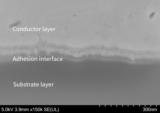
Cross-sectional SEM image of the adhesion between the substrate and the conductor layer
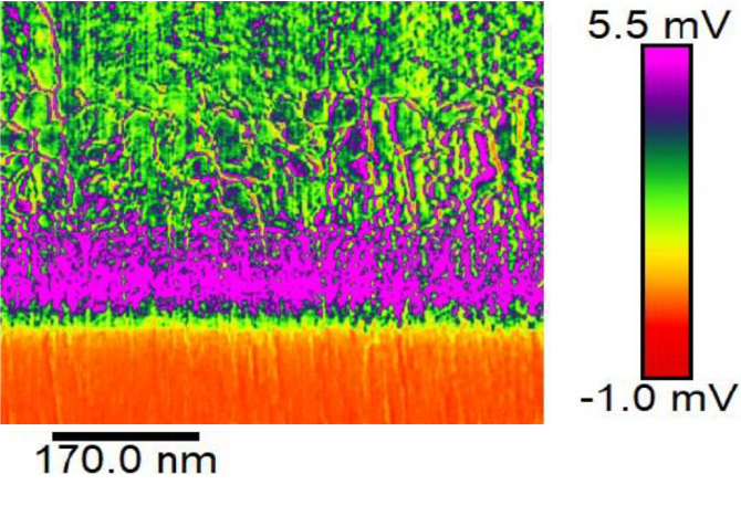
AFM-IR measurement results: Specific molecular bonding spectra extracted and mapped to identify atomic states at the conductor-substrate interface