

Core Technology
Backed by a team of over one hundred scientists and engineers, our R&D drives rigorous technological breakthroughs and ensures that each discovery is seamlessly translated into high-performance manufacturing.
-
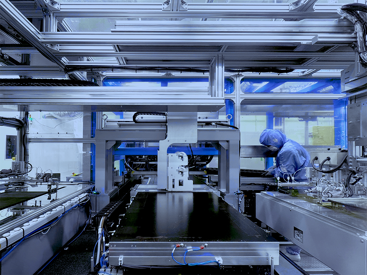
Precision inkjet printing
The inkjet equipment lineup deliver state-of-the-art performance and productivity for electronics manufacturing.
-
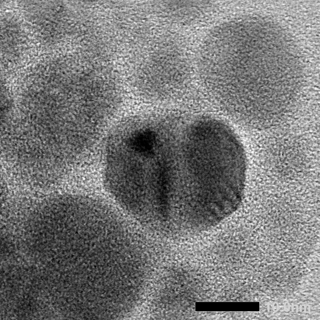
Materials
Advanced materials essential to the additive manufacturing process are researched and developed in-house.
-
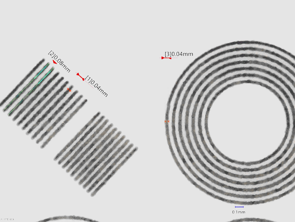
NeuralJet™
A high-precision inkjet technology enabled by control systems and AI-driven optimization.
Technical Articles
Elephantech Has Developed SAphire™ B: A Low-Resistance Copper Nanopaste for Inter-Board Connections in High-Layer-Count PCBsAchieves High Reliability Through Low-Temperature Sintering in Ambient Atmosphere
Elephantech announced SAphire™ B, a copper nanopaste designed for inter-board connections in advanced multilayer PCBs.
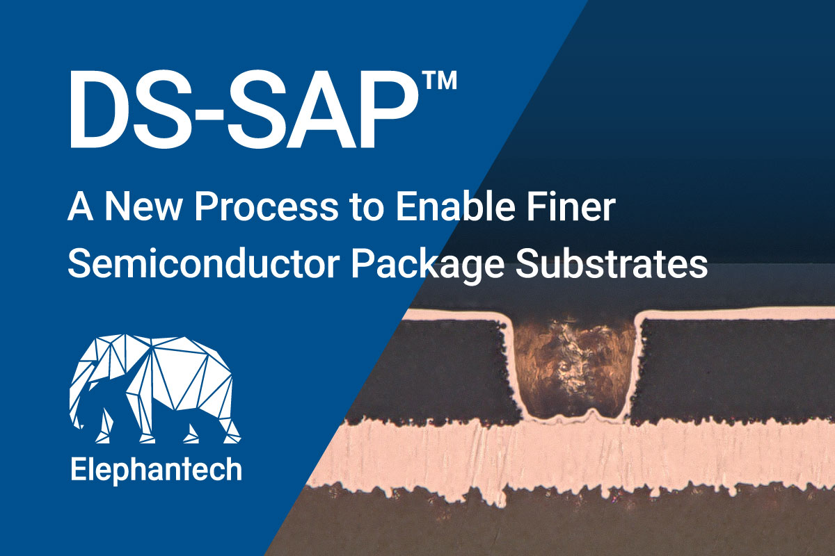
Elephantech Introduces DS-SAP™ for Fine Patterning on Semiconductor Package SubstratesDual-Seed Technology Enables Higher Density for Advanced AI Packaging
Elephantech has developed DS-SAP™, a novel process for semiconductor package substrates manufacturing. Through independently forming seed layers for surface patterning and via metallization, DS-SAP™ achieves both ultra-thin traces and reliable coverage of high-aspect-ratio vias.
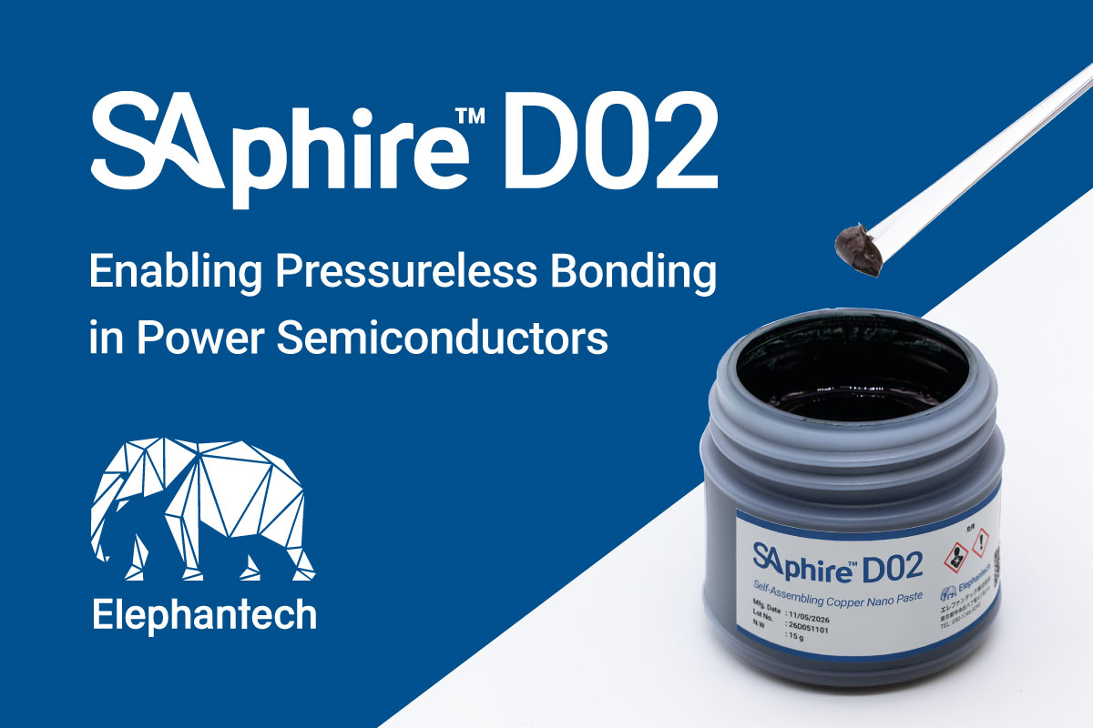
Elephantech Has Developed SAphire™ D02, A Copper Nano-paste for Pressureless Die Attach in Power SemiconductorsAdvancement of its Low-Temperature Sintering Technology Enables Greater Process Flexibility
Elephantech announces the development of SAphire™ D02, a new addition to its SAphire™ low-temperature sintering copper nano-paste lineup, designed for pressureless die attach applications.
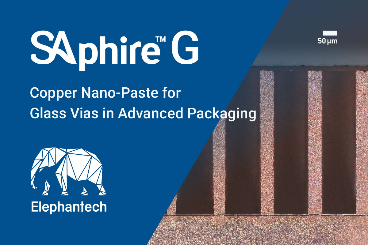
Elephantech Has Developed Copper Nano-Paste
SAphire™ G for Glass Vias in Advanced PackagingLow-Shrinkage and Robust Metallization for High-AR TGVs
Elephantech Inc. has developed "SAphire™ G," a copper nano-paste for Through-Glass Via (TGV) filling, utilizing its proprietary Self-Assembling Copper Nanoparticle (SA-CuNP) technology.
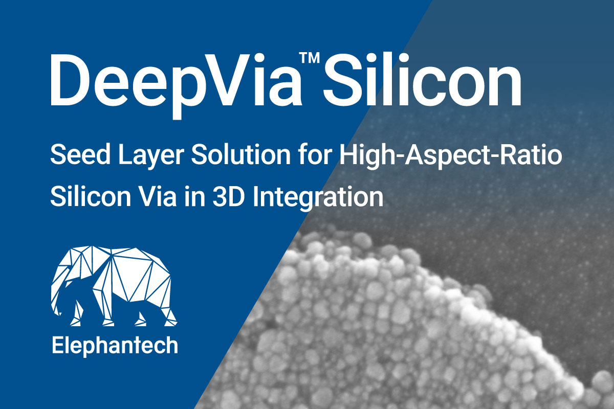
Elephantech Develops DeepVia™ Silicon: A High-Aspect-Ratio Seed Layer Solution for 3D Semiconductor IntegrationA Novel Approach for Silicon Via Seed Layer Formation Addressing Increasing Aspect Ratios
Elephantech has developed a novel approach for forming copper seed layers in high-aspect-ratio (AR) silicon vias, utilizing proprietary copper nanoparticle ink and inkjet printing equipment.