
Nano Copper Deposition
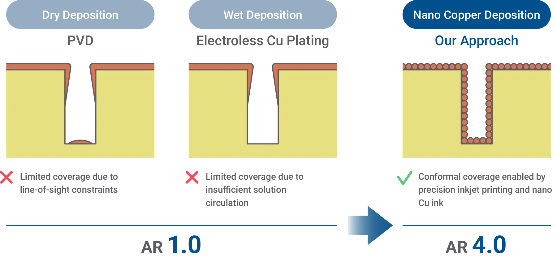
A fundamentally new approach to copper deposition, powered by inkjet technology and copper nanoink.
By selectively and precisely forming or augmenting seed layers only where needed, Nano Copper Deposition enables reliable seed coverage in challenging high-aspect-ratio structures.
It opens new possibilities for AI hardware manufacturing through greater routing flexibility, simpler processes and improved yield.
Our Solutions
DeepVia™ HDI
DeepVia™ HDI breaks the aspect-ratio barrier in HDI microvia metallization by forming continuous, conformal seed-layer coverage beyond constraints of electroless plating.
It enables precise control of via depth, reducing build-up requirements and supporting enhanced signal integrity in high-layer-count AI server boards.
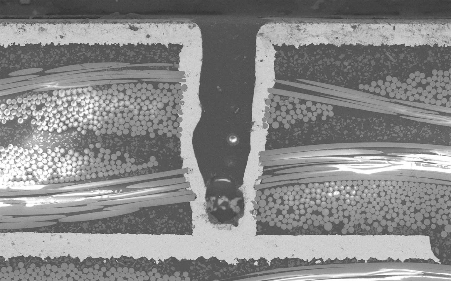
DeepViaTM HDI actual sample with aspect ratio of 3.0

Illustration of DeepViaTM HDI process flow
DS-SAP™
Dual Seed-SAP™ is a novel process that decouples surface fine-line patterning from deep-via metallization, eliminating the inherent process trade-off.
By enabling skip vias, DS-SAP™ reduces pad and keep-out area as well as build-up layers, significantly enhancing fan-out efficiency in advanced packages.
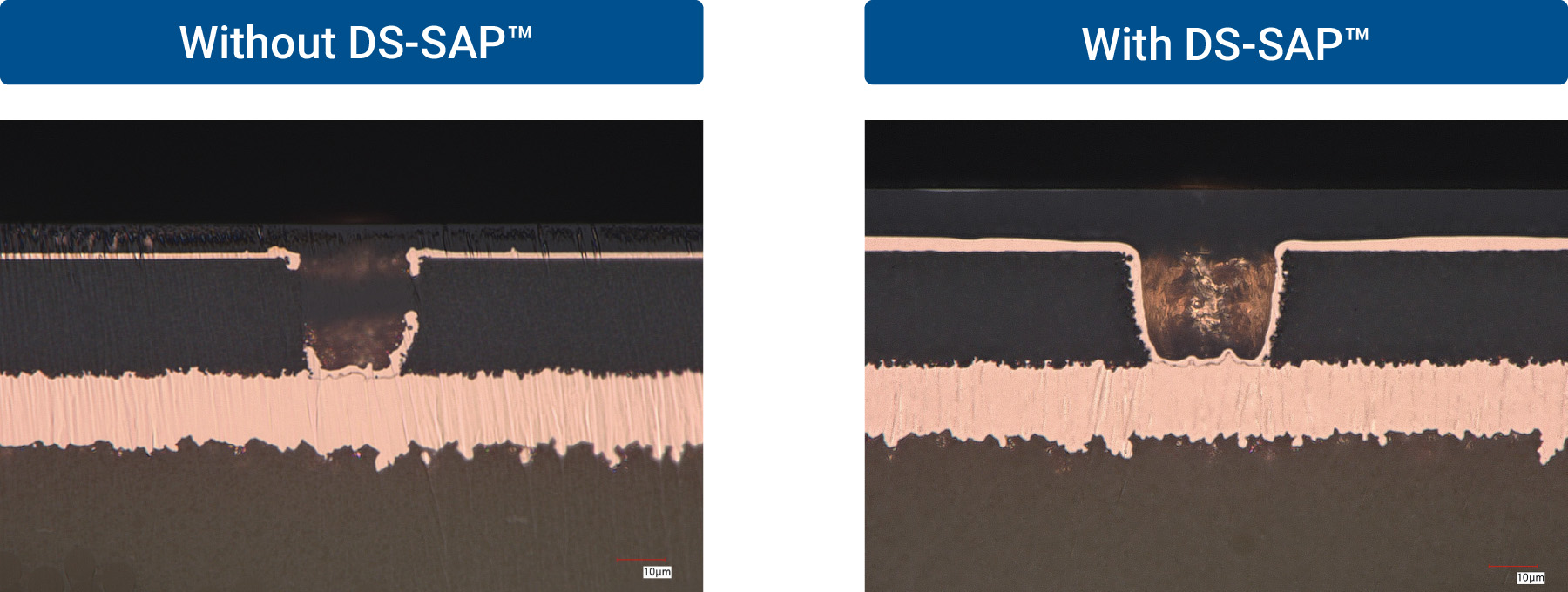
Comparison of via metallization with and without DS-SAPTM
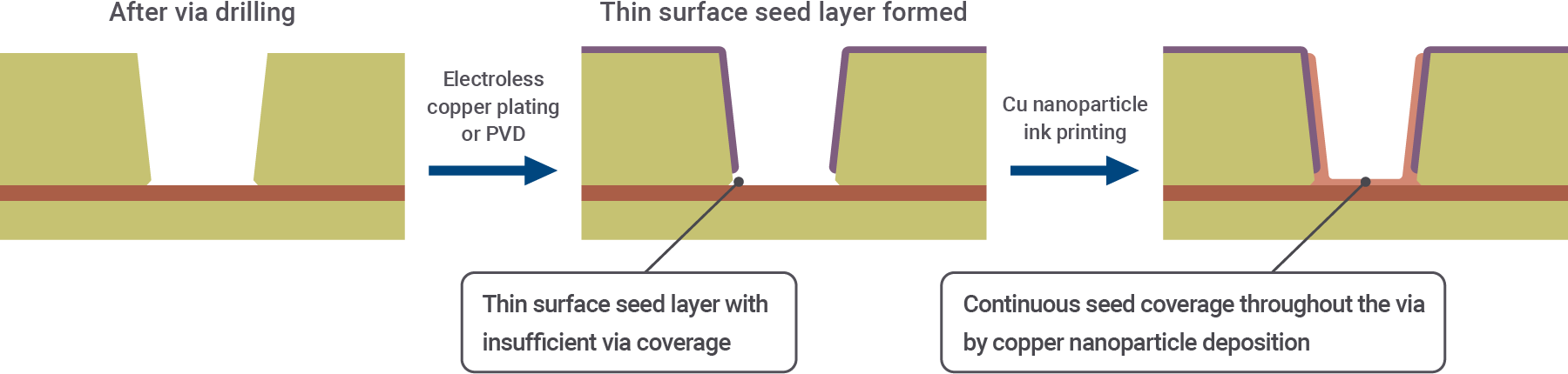
Simplified illustration of DS-SAPTM process flow
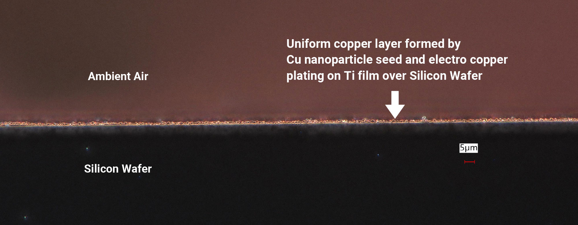
DS-Silicon™
DS-Silicon™ achieves conformal seed-layer coverage as silicon interconnects become smaller, deeper and more three-dimensional, overcoming the limitations of PVD.
It works as a standalone approach or complement existing PVD through a hybrid approach, expanding metallization capability for next-generation HBM/3D integration.
Cross-section of a DS-Silicon™ sample showing conformal copper coverage

Illustration of DeepViaTM Silicon process flow