
SustainaCircuits
SustainaCircuits is a PCB manufacturing technology built on Elephantech’s Nano Copper Deposition platform.
By forming conductive patterns through a fully additive approach, it helps reduce material consumption, process complexity, and environmental footprint.
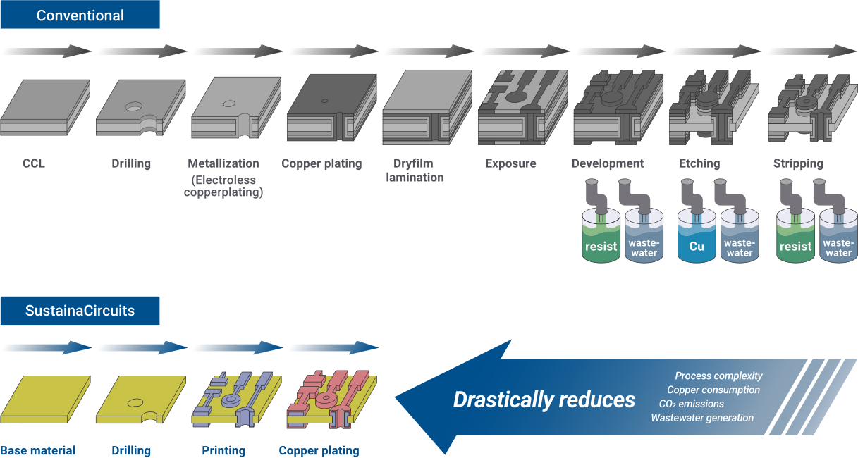
Manufacturing Process
SustainaCircuits uses inkjet printing to directly form the seed layer for circuitry patterns on the base materials, followed by reduction and electrolytic copper plating to build the conductors to the required thickness.
It delivers performance comparable to PCBs fabricated using conventional subtractive processes, while eliminating chemical-intensive steps.
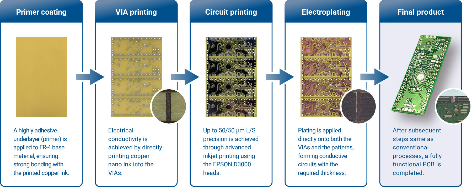
Key Benefits
SustainaCircuits’ efficiencies contribute not only to carbon footprint reduction but also to leaner operations and long-term cost performance, making it a forward-looking solution that aligns innovation with sustainability.
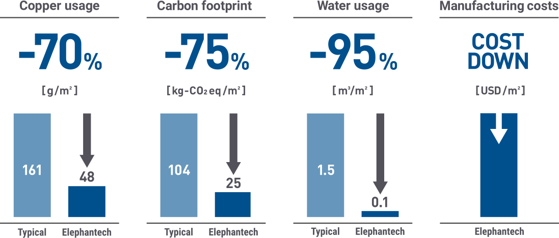
Calculation specification: 6-layer rigid PCB with board thickness of 0.8 mm and copper thickness of 35 µm [unit: kg-CO2eq/m2]